Characterization
About
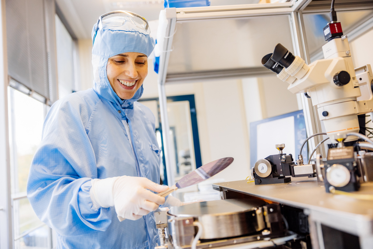
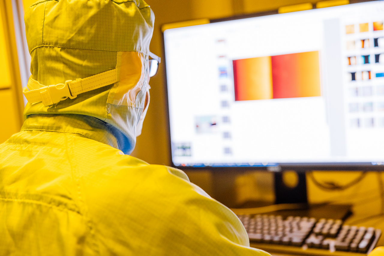
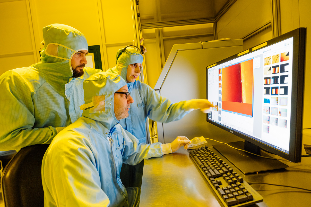
AMO runs a class 10 to class 1000 cleanroom with a total area of 400 m². High-end production facilities for semiconductor technology are operated here in a highly flexible manner to enable high-quality nanofabrication together with material and device characterisation for rapid process changes and unconventional solutions. All of the equipment described below is available to customers and partners as part of our services.
Description
Technical specifications:
| Type | Name | Technical Specifications |
| Scanning Electron Microscope (SEM): | ZEISS Supra 60VP | Up to 8” Wafers |
| Ellipsometer: | 1. Philips PQ Ruby Spectral | · Automated Mappings on up to 8” Wafers
·Laser wavelengths of 632,1301 and 1541 nm. |
| 2. J.A. Woollam | · Single wafer processing on 6″ wafers
· UV-Vis wavelength |
|
| Optical Microscope | 1. Leica INM 100
2. Leica INM 300 |
Image capturing on up to 6″ and 8”wafers |
| Atomic Force Microscope (AFM) | 1. Veeco Dimension 3100
|
· High resolution STM, AFM, MFM on 6″ wafers |
| 2. Bruker Icon | · surface topography scan, electrical measurement, conductive measurement, KPFM, magnetic measurement, specific applications requires specific probes,
· on 8″ wafers · Scan Range: (100×100) μm² down to (500×500) nm² (recommended), up to 1024 pixels |
|
| Spectrometer
|
Bruker Lambda 1050 | · transmission and reflectance, max. 10×10 cm², min 3×3 cm² (2×2 cm² possible with holder), 10×10 cm²
· Spectral range: 200 – 2500 nm |
| Raman spectroscopy system:
|
Horiba | · Confocal setup, single points, 2D, 3D, on 6″ wafers
· 3 wavelengths of 532 nm, 633 nm, 785 nm, 50x & 100x objectives |
| Surface Profiler: | Veeco DekTak³ST | · z-resolution ~20nm
· vertical range 100A-1310kA |
| Electrical Probe Station
|
1. Cascade Microtech | · Semi-automatic High end Parameter analyzer for small signal DC nanoelectronic device testing |
| 2. Agilent | · high-temperature chuck up to 300 °C
· 8″ wafers · Agilent Precision impedance analyzer(4294A) · Agilent semiconductor parameter analyzer(4156B) · Agilent pA-meter (4140B) · Agilent Precision LCR-meter (4284A) |
|
| 3. Lakeshore CRX-6.5 | · Temperature Range 6K-350K, 3 and 4 DC probe needles on 2″ wafers and
· Temperature Range 10K-650K, 3 DC probe needles, with optical fiber, on 2″ wafers |
|
| Optical-measurements setup | Silicon Photonics device testing on 8″ wafers | · Tunable laser;
· Fiber & butt coupled, · at 1300 nm and 1550 nm. |
| RF Lab | Electrooptical device testing | · DC and RF,
· on 8″ wafers |
Access Provider / Facilities