PARTNERS

  • ACCESS PROVIDERS
  • CLUSTERS

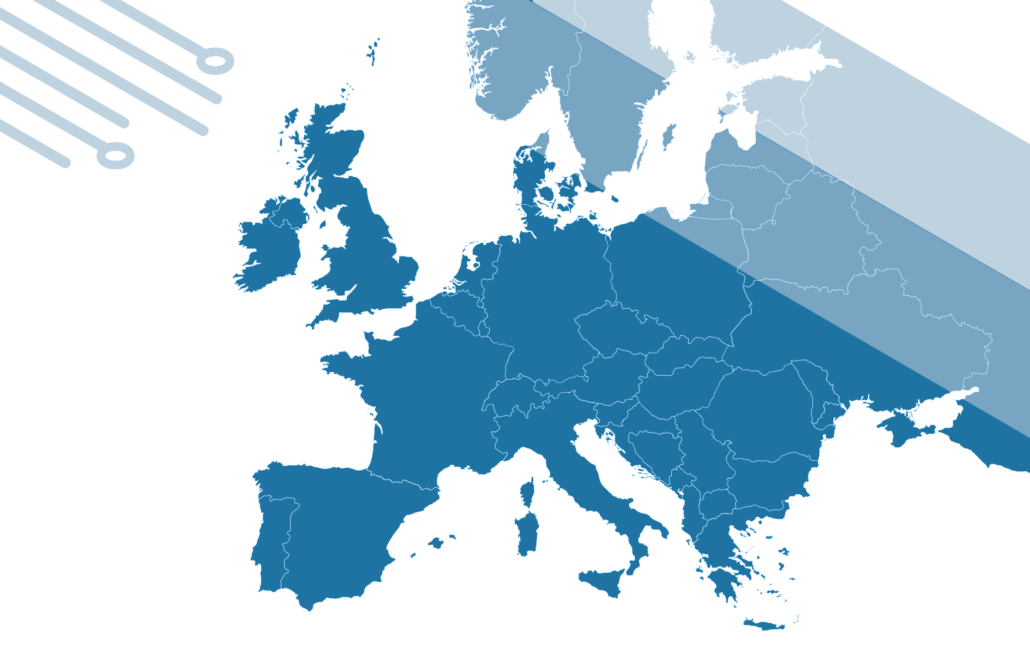
The INFRACHIP consortium is a combination of leading European research infrastructure, industry cluster organisations and knowledge hubs that will deliver an integrated Research Infrastructure for the semiconductor field. It consists of partners from Ireland, France, Greece, Germany, Portugal, Poland, Austria and Sweden. The consortium as a whole brings together the unique infrastructure, advanced equipment, state-of-the-art technologies and world-leading expertise required to deliver the ambitious objectives of INFRACHIP.

Tyndall National Institute

Cork, Ireland

Tyndall National Institute is a leading European research centre in integrated ICT hardware and systems. Central to Tyndall’s mission is delivering economic impact through research excellence. Tyndall works with industry and academia to transform semiconductor research into products in the core market areas of communications, agri-tech, energy, environment, and health. As Ireland’s largest research institute, Tyndall hosts over 600 researchers, engineers and support staff, including over 150 full-time postgraduate students, together generating over 200 peer-reviewed publications each year. Tyndall is home to Ireland’s hightech semiconductor research infrastructure, hosting the only full CMOS, MEMS and III-V wafer semiconductor fabrication facilities and services. With a network of 200 industry partners and customers worldwide, Tyndall generates 85% of its income from competitively won contracts

  • A 750m2 ISO7/ISO5(litho) ‘FlexiFab’ that allows for agile wafer scale nanofabrication and processing beyond silicon, and for experimenting with the integration of selected new materials and architectures aiming at enhanced device performance and added functionality. 
  • Building blocks for energy-efficient electronics and future computing architectures.
  • Hybrid integration of heterogeneous semiconductor chips for rapid (sub-)system prototyping – heterogeneous chiplet integration and packaging (flipchip single chiplet and design rules) and micro-transfer printing (mass chiplet transfer). 
  • Atomic Layer Deposition (ALD) and metallorganic vapour phase epitaxy (MOVPE).
  • Materials and device processing (2D transition-metal dichalcogenides, multiferroics and semiconductor oxides…)
  • Design and implementation of ultralow-power management integrated circuits for microprocessors in Internet of Things devices.
  • Development of new tool capabilities for wafer fabrication. Tyndall is also developing metrology processes, e.g., Scanning Capacitive Measurements (SCM) and Scanning Spreading Resistance Measurements (SSRM) for 2D mapping of dopants at the nanoscale, complemented by nanoscale device forensics. 
  • Process capability, simulation model expertise and platforms & infrastructure for metrology & benchmarking of energy harvesting power WSN (wireless sensor network) solutions

HMU: Hellenic Mediterranean University Research Center (HMU-RC)- Institute of Emerging Technologies (i-EMERGE)

Heraklion, Greece

HMU-RC was established in 2019, aiming to create a one-stop research facility housing all the HMU scientific & technological disciplines through six research Institutes. HMU-RC’s mission is to perform forefront research and to promote innovation and competitiveness for the benefit of society. 

i-EMERGE of HMU-RC is a multidisciplinary research institution focusing on frontier science and technology of cutting-edge materials and production processes with the potential to enable sustainable technologies to enhance citizens quality of life with economic benefits. There are currently four research divisions: Nanotechnology and Printed Electronics; 3D-Printing and Additive Manufacturing; 5G and Internet of Things applications, each of critical mass, which embrace the full spectrum from fundamental science to applied engineering and Neural circuits in Health. 

The Nanotechnology Division (Nano@HMU) of i-EMERGE leads the Energy Generation activities of the FET-Graphene Flagship initiative, while it participates in the newly established European Research Infrastructure “Emerging Printed Electronics and Photonics”, EMERGE, the European Perovskite Initiative and in the Advanced Technology Higher Education Network (ATHENA). Nano@HMU is working at the frontiers of nanoscience and solution-processed advanced materials towards the industrialization of emerging printed electronics and energy harvesting/storage devices. NANO@HMU is renowned for its achievements on interfacial engineering of emerging solar cells, such as perovskite and organic, for improved performance and stability, and on evaluating their performance in IEC certification tests at outdoor conditions and by using accelerated ageing ISOS protocols. The Nano@HMU has superior know-how on the formulation and printing of solution processable graphene and other 2D related crystals, as well as on their functionalization and doping for fine tuning of their energy levels and work-function.

  • Graphene and related 2D layered materials. 
  • Organic & perovskite solar cells. 
  • Industrialization of emerging PVs. 
  • Printed (2D/3D) & Flexible electronics. 
  • Internet of Things applications

The Nano@HMU team is one of the founding partners of RI EMERGE. Within EMERGE, Nano@HMU offers various TAs covering a wide range of installations including activities on inks/pastes formulation and material characterization, as well device (focusing on 3rd generation PVs) performance evaluation and standardisation.

NCSRD: National Center for Scientific Research “Demokritos” – Institute of Nanoscience and Nanotechnology

Athens, Greece

NCSR “Demokritos” is the largest research organisation in Greece comprises five Institutes: the Institute of Nanoscience and Nanotechnology (INN), the Institute of Nuclear Science and Particle Physics, the Institute of Biological Applications, the Institute of Information and Telecommunications and the Institute of Radiological protection, Energy and Safety. INN is the largest ICT research institute (80 researchers) with research priorities in the areas of Micro Nano Systems, Photonics and Microsystems. INN addresses topics in 5 KETs (Key Enabling Technologies): Nanotechnology, Advanced materials, Micro- and nano-electronics, Photonics, and Advanced Manufacturing Technologies. 

INN-NCSRD has extensive fabrication cleanroom facilities (Nanotechnology & Microsystems Laboratory, NML) in nanoelectronics (Si, 2D materials), photonic devices and MEMS, which are fully supported by extensive test and characterization facilities at a single site. The research activities of INN are based on the principles of “More than Moore” wafer processing with “Beyond CMOS” concepts with an emphasis on interdisciplinarity and technological convergence. INN has experience to provide services since was member of the first transnational access EU project IST I3 ANNA (2007-2010), as well as member of the first Network of Excellence in nanoelectronics, FP7-IST-NoE NANOSIL (2008-2011). In 2012, an advanced e-beam lithography tool was installed in INN funded by MINASYS FP7 EU-REGPOT project. Since 2017, INN has been coordinating INNOVATION-EL, the Greek Infrastructure Network for Nanotechnology, Advanced Materials and Micro/Nanoelectronics. INN is a single-site research institute enabling extensive interfacing between the NML and other activities across the microelectronics value chain in materials, devices and system integration.

  • Test & Characterisation (EH, ATS, CIM…)

CNRS: FMNT

Grenoble, France

FMNT is a research federation of the French National Research Centre (CNRS) grouping together seven laboratories (> 300 researchers) in the Grenoble area, with major research activities in microelectronics and micro-nanotechnologies. The research activities within the FMNT are structured around five strategic axes: microelectronics, components and systems for telecommunications, integrated measurement devices, components and systems for bio & health, materials and components for energy. Through its laboratories, the FMNT has important human resources and facilities. Some of this equipment are pooled in a dedicated platform named OPE)N(RA relating to functional characterization of materials and devices.

OPE)N(RA allows addressing electrical characterizations, for some combined with measurements under magnetic field (0 – 9T), mechanical stress (for MEMS/NEMS applications), temperature (2K – 1000K). Electrical characterizations sweep the frequency ranges from DC to a few hundred GHz. Some equipment is very low noise, others allow to work with controlled light source. Some of these equipments can accommodate 300 mm or 200 mm wafers or smaller scale devices. Anechoic chambers are dedicated to equipment for telecom applications. A wide range of equipment is also dedicated to photonics through characterization or prototyping and packaging. Other peripheral facilities are also available for a more material oriented analysis (Raman, XPS, ellipsometer…).

  • Test & Characterisation

Instituto de Desenvolvimento de Novas Tecnologias – UNINOVA

Caparica, Portugal

UNINOVA is a R&D institute organised in centres of excellence, involving >200 researchers, participating in this EU infrastructure through the Center of Excellence in Microelectronics, Optoelectronics and Processes (CEMOP). CEMOP integrates the Institute for Nanostructures, Nanomodelling and Nanofabrication (i3N, www.i3n.org), an Associated Laboratory since 2006 and one of the leading Portuguese institutions in the area of nanoscience and nanotechnology. The institute is strongly committed to UN 2030 Agenda for Sustainable Development and its activities are in line with the EU Green Deal approach, taking nanotechnologies and advanced functional materials to a broad range of cross-cutting fields, seeking to enhance the quality of life and to achieve sustained economic and citizens benefits. 

R&D follows 4 main thematic areas: Sustainable Micro and Nanofabrication; Green and Clean Energy Systems; Nanomaterials Engineering and Functional Interfaces; Biomedical devices and systems. For more than 25 years CEMOP has been coordinating and participating in several national and international projects with academia and industry, in the field of optoelectronic sensors, biosensors, solar cells, thin-film transistors and integration of such components. In these R&D activities, CEMOP researchers have been exploring materials and processes away from silicon to conceive devices and systems on rigid or flexible substrates.

 The group has a worldwide reputation for its pioneering work in transparent electronics and paper electronics. It holds 52 granted plus 19 pending patents in the field of advanced functional materials, devices and systems. The excellence of the multidisciplinary research team has been evidenced by the award of highly competitive funds, such as 10 ERC grants. The external international panel of evaluation of the Portuguese institutes considered the institute ‘a model of European Excellence and quality in the area of electronic materials, optoelectronics and microelectronics’. CEMOP has state-of-art infrastructures for fabrication, characterization and simulation of thin-film optoelectronic devices for flexible applications.

  • Materials synthesis – hydrothermal synthesis of oxide and metallic nanostructures, ink formulation, solution combustion synthesis; 
  • Device/prototype fabrication – split in two areas: 
  1. >400 m2 clean room space suitable for demonstrators up to 4” size, including substrate preparation, thin film coating by PVD (sputtering, evaporation), CVD and ALD tools, lithography with UV aligners, direct laser writer and nanoimprint, wet and dry etching and post-processing (RTP with different environments). 
  2. Printing lab with ink-jet, screen and flexoprinting, spray coating, spinners, shear casting and drop casting methods, glove boxes 
  • Material/device characterization – wide range of tools for electrical, optical, structural, chemical and morphological evaluation of materials and devices, including STEM, SEM/FIB with EDS, EBSD, EBIC and in-situ electrical characterization, XPS, micro-Raman, spectroscopic ellipsometry, temperature, light and environment-dependent IV and CV measurements, XRD, DSC/TGA, among many other possibilities. 
  • Design and simulation – tailored for design/simulation of oxide TFT circuitry in Cadence environment, as well as physical-level simulation of devices in Silvaco TCAD and Ansys Lumerical suites;

INL: LABORATORIO IBERICO INTERNACIONAL DE NANOTECNOLOGIA

Braga, Portugal

The International Iberian Nanotechnology Laboratory (INL), located in Braga, Portugal, is home to a micro- and nanofabrication facility that is the largest in Portugal for research and includes some of the most advanced instrumentation on the Iberian Peninsula. The core of the fabrication facility is housed in a 1200 m2 cleanroom: Class 100 in the lithography bays and Class 1000 in the other areas. The unique combination of tools and expertise for deposition, patterning, and etching of a broad range of materials enable extensive in-house capabilities for producing electronic, magnetic, optical, or MEMS devices as well as various “hybrid” combinations, e.g., MEMS structures functionalized with magnetic sensors or optomechanical MEMS devices. All of these fabrication processes are implemented at 200-mm wafer scale. Additional heterogeneous integration capabilities include structures that combine bottom-up and top-down methods for (self)organisation and patterning of nanomaterials and nanostructures. These fabrication capabilities are supported by in-house expertise on process design and integration as well as by a comprehensive suite of nanocharacterisation instruments and expertise, where the electron microscopy and spectroscopy facility plays a key role with 7 pieces of equipment (including SEM, TEM/STEM, DualBeam FIB-SEM or XPS).

  • Design
  • Fabrication
  • Characterization

JOANNEUM RESEARCH – MATERIALS (Institute for Sensors, Photonics and Manufacturing Technologies)

Weiz, Austria

JOANNEUM RESEARCH is a successful national and internationally active research institution owned by the Austrian federal states of Styria, Carinthia and Burgenland. Ideally embedded in the national and international innovation network, our researchers innovate in three high-level fields of expertise: “Information and Production Technologies”, “Human Technologies and Medicine”, and “Society and Sustainability”. At our seven institutes we use our ideas, innovative power and considerable research experience to support companies both private and public not only with the development of technology, methods and products, but also with societal topics.

JOANNEUM RESEARCH’s institute MATERIALS, located in Weiz, has long standing experience in managing a wide range of research cooperation, thus enabling the clients to successfully participate in national and international funded research projects. The team of around 90 researchers provides interdisciplinary solutions across the entire value chain – from the idea to the prototype – using cutting edge technologies and methods based on miniaturisation, integration and materials optimisation. Combined with state-of-the-art fabrication facilities and characterisation infrastructure, MATERIALS offers innovative solutions and services tailored to the needs of business and industry. The institute runs a 150m2 ISO14644 certified class 6 cleanroom, equipped with e-beam-lithography, photolithography and reactive ion etching. MATERIALS provides access to the latest technologies required for implementing innovative products and services.

  • Sensorics, Connectivity, Sustainability, 
  • Test & Characterisation
  • Sustainable sensors, advanced sensing technologies, RF components, short range optical communications 
  • Sustainability and green electronics

Myfab Chalmers , Chalmers University of Technology

Gothenburg, Sweden

Chalmers University of Technology conducts research and offers education in technology, science, shipping and architecture, with a sustainable future as its global vision. Chalmers is well-known for providing an effective environment for innovation and has eight priority areas of international significance – Built Environment, Energy, Information and Communication Technology, Life Science, Materials Science, Nanoscience and Nanotechnology, Production, and Transportation. Situated in Gothenburg, Sweden, Chalmers has 11,000 full-time students and 3,000 employees. Chalmers is the host of Myfab the national research infrastructure for micro and nano fabrication. Myfab has cleanroom nodes at Chalmers, The Royal Institute of Technology, Lund University, and Uppsala University.

The local node, Myfab Chalmers, offers a broad platform for micro- and nanofabrication with approximately 190 tools in operation in our 1250 m2 cleanroom facility. Two especially strong areas of expertise are in microwave- and photonic components and quantum components. Both areas rely on the strength and strong heritage within nanolithography. The staff consists of technicians, research engineers and senior research engineers, in total 21 persons. The cleanroom staff is responsible for the service and maintenance of the whole infrastructure including the facility. The infrastructure is used by more than 200 individuals annually, approximately 85 % come from academia and 15 % come from industry. The infrastructure is in the middle of a five year long reinvestment period where we invest approximately 175 MSEK in 34 new tools, where half of them replace outdated tools and the other half provide new techniques and capabilities.

  • Cleanroom fabrication for Power electronics, Quantum and Spin Devices, High frequency Components and more.

AMO GmbH

Aachen, Germany

The research foundry AMO GmbH is a non-profit SME specialising in R&D for micro- and optoelectronic applications. AMO acts as a pathfinder for innovative technologies for nanoelectronics and nanophotonics applications for the German and European industry. The mission is to demonstrate innovative technologies and to introduce new materials, including their implementation in novel device architectures, prototyping and small volume fabrication. A broad base of advanced semiconductor process technologies is available. 

As a research oriented company, AMO efficiently closes the gap between university research and industrial applications. For this purpose, AMO identifies those topics from basic research that seem particularly suitable for industrial implementation and demonstrates these in application oriented technology. In parallel to applied research, AMO engages in groundbreaking research in several FET Open and similar low TRL projects that lay the foundation for high TRL research and transfer to larger industry at a later stage. 

One of the main activities at AMO falls within research on More Moore and Beyond CMOS devices in cooperation with leading European academic and industrial partners. The current focus lies on electronic and opto-electronic devices based on two dimensional materials. The strength of AMO lies in the implementation and demonstration of novel devices and architectures at a prototype level. The team has long-standing expertise in nanoelectronic devices, from nanowire / FinFETs to ultra-thin body SOI. Research on new material has led to the demonstration of high-k / metal gate integration. In recent years, AMO has become a global player in 2D materials research for electronics and photonics. 

AMO hosts the Advanced Microelectronic Center Aachen (AMICA), a 400m² clean room facility with a large installed base of equipment for semiconductor process technology, including electron beam lithography, optical contact lithography and an i-line stepper, several nano-imprint lithography tools, interference lithography, a thermal evaporator, sputter deposition, two ALDs, three dry etching chambers, various furnaces etc. The equipment is centred on the silicon platform with a long CMOS history, but has been carefully extended in the recent years towards new materials.  

  • Advanced sensing
  • Photonic sensing
  • Neuromorphic computing
  • RF components & Design

WUT & CEZAMAT: Warsaw University of Technology – Centre for Advanced Materials and Technologies

Warsaw, Poland

Warsaw University of Technology (WUT) is the largest and one of the best universities in Poland involved in scientific and research activities in applied science in nearly all technical areas. Research and development work conducted at WUT meets the challenges of modern science and the economy. Centre for Advanced Materials and Technologies CEZAMAT of Warsaw University of Technology is one of the greatest investments in Poland in the area of high technologies. CEZAMAT addresses topics in 5 KETs (Key Enabling Technologies): Nanotechnology, Advanced Materials, Micro- and Nano-electronics, Photonics, and Advanced Manufacturing Technologies. 

CEZAMAT is a unique research centre that enables interdisciplinary research on future-oriented materials and technologies. The main goal of CEZAMAT is to provide a platform that will integrate the research community and enable the development of interdisciplinary research. CEZAMAT collaborates with Polish and international scientific communities and companies that use innovative technologies and products. The laboratories of CEZAMAT are the most advanced and the largest of their kind in Poland. These laboratories include almost 4000 m2 of cleanroom space (suited for both semiconductor and bio-oriented research).  

Centre for Advanced Materials and Technologies CEZAMAT of Warsaw University of Technology is carrying out R&D in nanotechnology, biotechnology, printed electronics, microelectronics and photonics, emphasizing novel nano-electronic sensors and devices, energy harvesters and photonic integrated circuits. The state-of–art laboratories of CEZAMAT allow the development of new marketable technologies with commercial potential, which are supposed to contribute to economic development. WUT-CEZAMAT is a member of European associations: EPoSS, AENEAS.

  • Design, Modelling & Simulation 
  • Test & Characterisation a
  • Advanced Sensing Technologies, 
  • Sustainable Sensors
  • Energy Harvesting

SiNANO Institute

Grenoble, France

The SINANO Institute is the European Academic and Scientific Association for Nanoelectronics, acting as a network of excellence connecting the European Research and Academic community in semiconductor science and technologies. It gathers 26 academic/RTO and members in the area of fabrication, characterization, modelling, design and simulation of emerging nanoelectronic materials, devices, circuits and systems from 16 European Countries. Recently, 22 deeptech Start-ups were connected to SINANO community.

The SINANO Institute was established in 2008 following the request of the European Commission at the end of the very successful Network of Excellence SINANO. Since then, its mission is to secure the future of European semiconductor science and technology by mobilising and nurturing the European Research and Innovation community, promoting and strengthening synergies in the field through our membership, accelerating the translation of excellent research into European knowhow, technologies, and products together with our start-ups and industrial partners, ensuring the pipeline of talented researchers and the growth of skilful talent in an inclusive and diverse environment with equal opportunities for all. In this framework, the SiNANO Institute organizes large-scale events, specialised workshops, webinars, Summer Schools and dedicated Young Researchers events.

Members of the Institute are particularly exploring disruptive science and technology aspects to identify the most promising topics for future ICT and speed up technological innovation. Activities from More Moore, More than Moore, Beyond CMOS, covering Sustainable Electronics, Smart Systems and System Design are sound competences of the SiNANO Institute’s members.

The SiNANO Institute is also organizing international Workshops and Conferences to develop high competence levels in Europe, and participating in roadmap definition. In this respect, the Sinano Institute is the European representative of IRDS “International Roadmap for Devices sand Systems”. SiNANO plays an important role in structuring European programmes and nurturing synergies in the European ecosystem. In collaboration with Research Institutes and Industry, SiNANO strengthens the overall innovation efficiency of the European research in Nanoelectronics.

SINANO has started to integrate the spin offs of its members to complete the innovation value chain of the SINANO Institute ecosystem – from renown universities and academic departments to mid-size research and technology infrastructures (Tyndall, VTT, INL, …) and to the start-ups/SMEs innovators. The SiNANO Institute ambition is to act as the early-stage research platform that fosters the next generations of Key Digital Technologies.

Silicon Saxony

Dresden, Germany

With more than 500 members, Silicon Saxony is the largest high-tech network in Saxony and one of the largest microelectronics and IT clusters in Germany and Europe. Since its foundation in 2000, Silicon Saxony has been a self-financed association linking manufacturers, suppliers, service providers, universities, research institutes, public institutions as well as industry-relevant start-ups in Saxony and beyond. The cluster’s focus is on technological trends of the present and future – e.g. artificial intelligence, robotics, automation, internet of things, sensors, energy efficiency as well as neuromorphic and edge Computing. As a high-profile information, communication and cooperation platform, the association promotes the regional, national and international networking of its members by participating in and organizing industry events. Moreover, Silicon Saxony is one of the founding partners of Silicon Europe – an alliance of twelve European clusters for advanced electronics and software technologies. Since 2012, the network bears the GOLD label for excellent cluster management by the European Cluster Excellence Initiative (ECEI).

Minalogic

Grenoble, France

Founded in 2005, the Minalogic Auvergne-Rhône-Alpes innovation cluster is the driving force behind digital transformation, serving the strategic challenges of reindustrialization, national sovereignty, and sustainable development.

With offices in Grenoble, Lyon, Saint-Etienne and Valence, Minalogic drives an ecosystem of nearly 500 members that includes more than 420 innovative companies from across the region that cover the entire digital technology value chain. Minalogic’s members also include 20 research and training organizations (bringing together more than 150 laboratories), local government, banks and investors to sustain a unique network dedicated to innovation in digital technologies.

Minalogic helps all of its stakeholders make business connections through targeted, qualified introductions and create opportunities to innovate and grow at the national, European, and international levels.

Drawing on the recognized expertise of its team, Minalogic’s services are based on three complementary missions:

  •       animating a regional innovation network on an international level,
  •       supporting innovation projects
  •       and valorizing the technological expertise of its ecosystem.

Since 2005, the cluster has certified and helped secure financing for 885 projects for a total of €1.14 billion in government funding and a total R&D investment of more than €2.7 billion. With a network of over 20,000 active contacts, the cluster has initiated nearly 3,000 targeted contacts and 12,600 B2B meetings since its creation.