Electron Beam Lithography
About
Electron beam lithography (EBL) is a versatile mask-less (“direct-write”) patterning technique based on the exposure of an electron-sensitive material (termed as resist) to a focused electron beam.
Description
Electron beam lithography (EBL) systems enable flexible and accurate pattern transfer at the micro/nanoscale via exposure of suitable e-beam resists. Following resist deposition on the sample and baking, the electron-beam is scanned over the sample, in accordance to the pattern designed by the user using appropriate CAD tools and corrected for process and electron-scattering (proximity) effects via lithographic data preparation software. Subsequently, the exposed or unexposed areas of the resist are selectively dissolved in a suitable solvent. This results in the engraving of the user-defined pattern or its reverse into the resist.
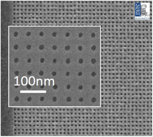
Depending on the EBL system and the exposed materials, sub-20nm feature resolution and accuracy in pattern positioning can be achieved. Unlike optical lithography which requires photomasks for pattern projection, EBL gives the user the flexibility to create, test and optimise various structures and patterns at the micro/nanoscale, before selecting the optimal solution for his needs.
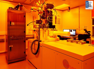
We offer access to the Raith EBPG5000plusES system operating at 100kV and allowing writing of sub-10 nm pattern features on substrates up to 100 mm (4”) in diameter.
Typical applications include high-resolution mask-less patterning for the development of Micro/Nanoelectronic, Quantum and Photonic multilayer devices, NEMS/MEMS, Greyscale (3D) structures, NIL stamps, metasurfaces, DOEs, holograms etc.
Technical specifications:
- Tool: Raith EBPG5000plusES
- Exposure: High current density thermal field emission gun for operation at 100kV, 25MHz writing frequency, 260μm writing field size, 100pA-220nA writing current range
- Resists: Positive/negative tone e-beam resists including bi-layers for lift-off applications.
- Pattern Resolution& Alignment accuracy: 8nm minimal feature size, field stitching accuracy: ≤15nm
- Sample Size: From 1x1cm2 samples to 100mm (4”) wafers
- Related Tools: Karl Süss RC8 & Headway EC 101D spin-coaters, High-precision hotplate (ATV), Software for lithographic data preparation (Layout BEAMER, GenISys), CAD tool for pattern design (K-Layout)
- Environment: Clean-room ISO 6 (Class 1000)
Case study:
INFRACHIP user investigates the feasibility of fabricating a Fresnel nanolens based on greyscale (3D) lithography. InfraChip user discusses the deliverable specifications with points of contact at NCSRD who assess its feasibility and supply the user with feedback on the modalities and parameters of fabrication, which involves EBL processing coupled with dry etching (RIE) for pattern transfer. The e-beam resist 3D topography that is accomplished by a suitable variation of EBL exposure doses, can be finely tuned to the actual etching rates during the pattern-transfer step.
The team of clean room engineers engage in the manufacturing process and its optimization, in vitro (use of tailor-made & commercial software for 3D pattern transfer simulation and calculation of lithographic parameters), and in vivo (actual testing and subsequent characterization of lithographic output). The fabrication process is quantified, developed, tested and optimized, resulting in the realisation of Fresnel lens prototypes.
The simulation of the pattern transfer process ensures minimal need for testing and can be applied to any type of 3D EBL application, whether it requires positive or negative tone e-beam resists.
(see G. Zisis et al., DOI:10.1016/j.mne.2022.100117)
Access Provider / Facilities