Ion Implanter
About
Implantation of atoms or molecules into a solid to modify its physicochemical properties. This technique is widely used for the fabrication of active electronic components like diodes and transistors.
Description
Ion implantation is a process of introducing in a controllable way energetic atoms or molecules into a solid to alter its physicochemical properties. Atoms or molecules are first vaporized and ionized, accelerated in an electric field, selected according to their mass-to-charge ratio and directed at the target material. Their penetration depth is determined by their mass, the acceleration energy, the target material including the crystalline state of the latter, and the angle of incidence of the ion beam. The dose (atoms/cm2) of the implanted species is controlled by monitoring the ion beam current. Selective implantation can be achieved by means of a patterned masking material (e.g., SiO2, Si3N4, photoresists) formed onto the surface of the target material.
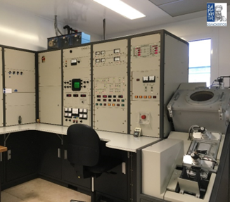
We offer access to the Eaton NV-3204 for implantation of elements like As, B, Sb and P at an energy in the 20-200 keV range into solid substrates of size up to 100 mm (4”) in diameter.
Introduction of dopant atoms is the most common application of ion implantation in the semiconductor industry. In that case a thermal treatment is applied after ion implantation to activate the dopant atoms (e.g., B, P, As for Si technology) and damage recovery of the crystalline lattice. In addition to Si, Ge and compound semiconductor doping for the manufacturing of a wide range of devices (e.g., diodes, MOSFETs, Bipolar transistors, MESFETs, JL-FETs), ion implantation is also employed for other applications including: Modification of insulating layers, fabrication of nanocrystals, modification of polymers and nano-composite materials, etc.
Technical specifications:
- Tool: Eaton NV-3204, Medium Current Medium Energy Ion Implanter
- Ion Energy: 20 – 200 keV (selectable in 1 keV increments)
- Ion Beam Current: Up to 500μΑ
- Species: B, BF2, P, As, N, Si, Ar
- Uniformity: Better than 0.75%
- Repeatability: Better than 0.5%
- Mass range: 125 AMU at standard extraction voltages
- Mass resolution: M/ΔΜ>100/1 (ΔΜ is the full width at half height)
- Implant Angle: Adjustable 0 to 15 degs
- Substrate size: From 100 mm (4”) wafer down to 1 cm x 1 cm samples
- Environment: Clean-Room (ISO 6 / Class 1000)
Case study:
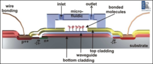
Our ion implantation facility has been successfully used for the development of a monolithic silicon microphotonic Mach-Zehnder Interferometer for biosensing applications. The main building block of this device is a monolithic optocoupler where light emitting diodes (LEDs) and silicon nitride planar waveguides are monolithically integrated and optically coupled on a silicon die. Thanks to our co-development approach, we have been able to identify and meet the user needs, especially regarding the fabrication of the LEDs (silicon avalanche diodes that emit white light when biased beyond their breakdown voltage). In that case the LED P++ emitter is implanted through the silicon nitride layer, the boron atoms compensate the preexisting base N+ implant so that the metallurgical junction of the LED is precisely placed under the up-going segment of the waveguide (see K. Misiakos et al., DOI:10.1364/OE.22.008856).
Access Provider / Facilities