Metal Evaporators
About
Metal evaporation is a versatile high-vacuum physical vapour deposition technique for producing metal coatings.
Description
Metal evaporation is used for manufacturing high-purity uniform single and multiple metal layers at a rate typically in the range of 0.1 to 10nm/s. The most widely employed methods are electron beam (also referred to as electron gun) evaporation and thermal evaporation. In the former case, a high-energy electron beam is used to heat the material to be deposited, which evaporates and condenses onto the substrate, while in the latter case, material evaporation is achieved via a resistively heated support.
As metal evaporation is a non-conformal deposition technique, it is ideal for lift-off processing. Ultra-thin multi-layers can be deposited via a multiple crucible system, with the ability to obtain gradient programmed compositions without breaking the vacuum. Metal evaporation is used in a wide range of applications, going from electrical contact engineering and interconnect lines in micro/nanoelectronics to transparent conductive thin films of designed reflective and transmissive properties in optoelectronics including photovoltaics, etc.
We offer access to both electron beam and thermal evaporation methods for a wide range of metals and their combination with a tight control over the thickness and composition of the deposited layers.
Technical specifications:
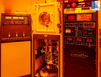
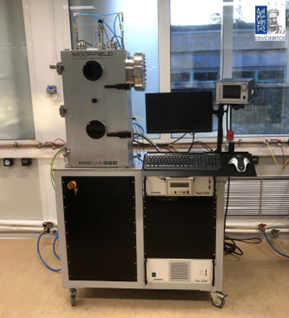
- Tools: 2 Evaporation Systems (ES) are available including,
(ES1) DENTON / DV-602, e-beam evaporation (1 pocket 7cc)
(ES2) Moorfield MiniLab 080A, e-beam evaporation (6 pockets 7cc each) & thermal
evaporation (1 pocket)
- Metals: (ES1) Al, (ES2) Al, Au, Ti, Cr, Pt, W, Ni, Fe
- Substrates: Semiconductors, dielectrics, resist coated and patterned substrates
- Evaporation Source:
(ES1) e-Gun 2kVA, capable of 400A (at 5V) or 200A (at 10V),
(ES2) e-Gun 5kW, capable of 10kV at 0 – 500mA emission current, Thermal Evaporation
Source: 200A / 8V.
- Deposition rate: (ES1) from 100 to 360 nm/min, (ES2) from 0.1 to 10 nm/s
- Substrate Size:
(ES1) From 1cm x 1cm samples to 100 mm (4”) wafers. Multi-wafer holder (up to
six 4” or six 3” wafers)
(ES2) From 1cm x 1cm samples to two 100 mm (4”) wafers, single 6” or 8” wafer.
- Environment: Clean Room Class 1000 (ISO 6)
Case study:
An InfraChip user discusses the possibility of EBL and pattern transfer on a charging substrate (quartz) via Aluminium deposition and its subsequent lift-off. The choice of a charging substrate will require a tailor-made process development approach that takes into account the charging effects present during the EBL step and in addition, will influence the choice of resist scheme to be employed for optimal lift-off. Clean room engineers investigate, test and develop a functional process which is compatible with the above charging substrate and the materials used.
The above non- fictional case-study describes the roadmap for the realisation of interdigitated gas and liquid sensors fabricated in our facility, via deposition and lift-off of thin Al films on quartz.
Access Provider / Facilities