Photonic Circuits and Devices
About
Silicon nitride passive photonic elements, integrated circuits and devices operating in the VIS-NIR (450-1100 nm) tailored for user-specific applications. Designs can include elements selected from the laboratory’s designs or defined by the users according to their specifications and requirements. We also offer our expertise for the co-creation of new photonics elements, devices and circuits. You design it, we create it for you.
Description
Photonic circuits, especially in the VIS-NIR range, are invaluable tools for high-precision, real-time sensing applications such as biodiagnostics, food safety and quality assurance, and environmental monitoring. Recent advances in micro/nanofabrication and emerging nanomaterials and nanostructures have enhanced the optical detection arsenal with disruptive and breakthrough nanophotonic tools that will form the basis for the next generation of optical sensing techniques and devices.
NCSRD, with long-standing experience in the design and fabrication of radical photonic elements and devices, offers its expertise and facilities for the development of photonic elements, devices, and circuits operating in the VIS-NIR range. Although our focus over the years has primarily been in the field of optical biosensing, we are keen to explore other applications and assist our users in designing and bringing their devices and circuits to life.
NCSRD’s expertise, flexibility and forward-thinking is materialized through the use of our 400m2 ISO-6 certified Si-processing Clean Room Facility, equipped with all the necessary pieces of equipment for the full process of silicon nitride-based devices.
Key equipment feature:
- Electron-beam Lithography Tool (Raith EBPG5000plusES system) with 8nm minimal feature size, field stitching accuracy of ≤15nm,software for lithographic data preparation (Layout BEAMER, GenISys) and CAD tool for pattern design (K-Layout). Both positive and negative lithography are possible.
- Optical Lithography Tools (both positive and negative tone capability) to complement e-beam lithography
- Furnaces and Low Pressure Chemical Vapour Deposition for annealing and oxidation and of silicon substrates as well as deposition of polysilicon and silicon nitride (SixNy) layers
- Dry Etching Systems
- E-beam Evaporator (Metal)
- Atomic Layer Etching
- High-resolution FE-SEM
Technical specifications:
- Sample size: from 2x2cm2 all the way to 4”Si wafers
- Customizable thickness of SixNy: 50-200 nm
- Customizable Photonic elements: planar waveguides (rib, ridge), tapers, MMI couplers, Interferometers (Mach-Zehnder and Young), microring resonators, grating couplers and photonic crystals
Case study:
FOODSNIFFER PROJECT
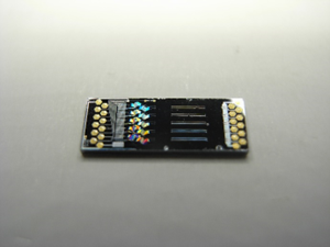
37mm2 fully-spectroscopic monolithic chip containing 10 integrated Si-based LEDs, 10 MZIs, 5 AWGs, and five 1×5 Photodiode Arrays for Point-of Need multi-analyte label-free sensing
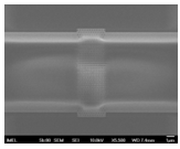
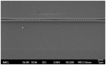
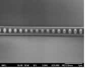
SUSPENDED Si3N4 OPTICAL CAVITIES
Optional:
K. Misiakos, E. Makarona, M. Hoekman, R. Fyrogenis, K. Tukkiniemi, G. Jobst, P.S. Petrou, S.E. Kakabakos, A. Salapatas, D. Goustouridis, M. Harjanne, P. Heimala and I. Raptis
All-Silicon Spectrally Resolved Interferometric Circuit for Multiplexed Diagnostics: A Monolithic Lab-on-a-Chip Integrating All Active and Passive Components
ACS Photonics 2019671694-1705 (2019), DOI: 10.1021/acsphotonics.9b00235
A. Christofi, G. Margariti, A. Salapatas, G. Papageorgiou, P. Zervas, P. Karampimperis, A. Koukourikos, P. A> Tarantilis, E.H. Kaparakou, K. Misiakos and E. Makarona
Determining the Nutrient Content of Hydroponically-Cultivated Microgreens with Immersible Silicon Photonic Sensors: A Preliminary Feasibility Study
Sensors 2023, 23 (13), 5937 (2023), DOI: 10.3390/s23135937
L. Athanasekos, A. Christofi, G. Gantzounis, E. Bolomyti, G. Papageorgiou, M.-C. Skoulikidou, I. Raptis, N. Papanikolaou,
Design and fabrication of suspended Si3N4 nanobeam cavities,
Microelectronic Engineering, 159, (2016), DOI: 10.1016/j.mee.2016.02.040
Access Provider / Facilities


