Ambient Pressure Photoemission Spectroscopy System APS04
About
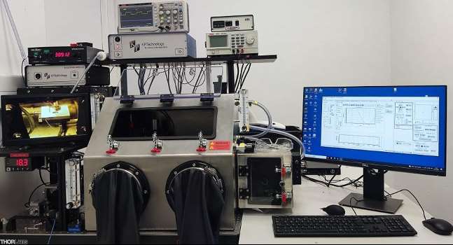
The APS04 system combines APS and high-resolution KP for fast semiconductor property analysis, including Fermi-level determination and surface topography mapping.
Description
The APS04 system combines two different techniques: Ambient pressure Photoemission Spectroscopy (APS) (absolute work function Φ/IE/HOMO) and high-resolution Kelvin Probe KP. APS + KP allows both the Fermi-level and valance band maximum/HOMO level of semiconductors to be rapidly determined. The APS system allows total photoelectron yield to be measured as a function of a tuneable DUV source. A second tuneable Visible/IR source is used to perform DC and AC white light Surface Photovoltage (SPV), and Surface Photovoltage Spectroscopy (SPS) measurements allowing Eg to be determined. Finally using the scanning Kelvin probe (SKP) the sample work function and surface topography can be mapped up to 50 x 50 mm2.
Technical specifications:
- Measurement Principle Photoelectric Effect: Energy Range 3.4 – 7 eV, Repeatability Precision 0.05 eV
- Work Function resolution 1-3 mV (2mm), 5-8 meV (50 μm)
- Maximum Sample Size 50 x 50 mm (2 x 2 inches
- Automatic Measurement of surface potential, DC-SPV.
- Relative Humidity Control Relative humidity chamber 25-80%
- Relative Humidity Resolution 1%
- Sample Temperature Control: RT-250 oC
Case study:
The versatility of the APS system, which allows total photoelectron yield measurements using a tunable DUV source, as well as DC and AC white light Surface Photovoltage (SPV) and Surface Photovoltage Spectroscopy (SPS) measurements with a second tunable Visible/IR source, empowers the user to comprehensively analyze semiconductor materials and accurately determine parameters like bandgap (Eg). The scanning Kelvin probe (SKP) capability of the system allows the user to map sample work function and surface topography with high resolution, providing valuable insights into material properties and surface morphology. INFRACHIP empowers the user to make significant strides in semiconductor research and innovation, driving forward advancements in the field.
Access Provider / Facilities


