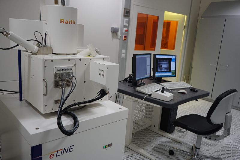
Electron beam lithography (RAITH/e-line)
About
Electron beam lithography (EBL) is a method for creating ultra-fine, nanometer-sized structures in modern nanotechnology. It is an important instrument in semiconductor technology, used to produce photomasks for photolithography, or stamps for other lithographic processes.
Description
The EBL is based on conventional scanning electron microscopes (SEM), but rather than scanning over the sample line by line as is the case for imaging, the beam path is defined by the desired structural geometry, thus writing information into surfaces. Accordingly, it is a very flexible, albeit time consuming, serial process. One major benefit of the EBL is its very high resolution, which is not limited by diffraction. EBL is used in semiconductor technology to produce nanostructures on silicon: for this purpose, the silicon is first covered with a thin layer of photoresist, which is then structured by the electron beam. The structured photoresist is partially removed by development and the inscribed pattern is subsequently transferred to the silicon through etching.
Technical specifications:
The EBL is based on conventional scanning electron microscopes (SEM), but rather than scanning over the sample line by line as is the case for imaging, the beam path is defined by the desired structural geometry, thus writing information into surfaces. Accordingly, it is a very flexible, albeit time consuming, serial process. One major benefit of the EBL is its very high resolution, which is not limited by diffraction. EBL is used in semiconductor technology to produce nanostructures on silicon: for this purpose, the silicon is first covered with a thin layer of photoresist, which is then structured by the electron beam. The structured photoresist is partially removed by development and the inscribed pattern is subsequently transferred to the silicon through etching.
Case study:
A user requires the fabrication of nanostructures to test new device configurations for their transistors. After the discussion with the Joanneum team, a strategy for the manufacturing is developed. For this silicon is first covered with a photoresist layer. After finding optimum setting for this configuration, then the structured is inscribed by the electron beam. The structured photoresist is developed so that the information is present in the polymeric layer. Finally, the structure is transferred to the silicon through etching and residual polymeric layers are removed.
Access Provider / Facilities