Electronic Component Packaging

About
The Tyndall Packaging Laboratory offers a comprehensive range of component assembly capabilities for microelectronic, microsystems & sensor components. Tyndall’s capability is a flexible low volume one aimed primarily at supporting the prototyping needs of industry users and research project partners.
Description
The packaging capability includes all of the processes required to take integrated circuits from the wafer and assemble them in a variety of packaged formats. The full packaging process available in the laboratory include: Ceramic Packaging, Chip-on-Board (CoB) assembly, Plastic (Glob-top) encapsulated assembly and Multi-Chip Module (MCM) assembly.
These processes are typically used in low-volume to build prototype devices for the validation of new technologies or the investigation of novel materials or assembly techniques. The facility supports the development of new IC & Microsystems technologies through the provision of a support service by which new devices may be quickly packaged for test and characterisation purposes.
The principal capabilities include:
– Lapping & grinding system to thin wafers & die to < 100µm (max wafer size = 100mm).
– Automatic wafer dicing saws (wafers of up to 200mm).
– Die ejection system (removal of individual ICs from thermal release dicing tape).
– Dispense system for deposition of die-attach adhesives & glob-top encapsulants.
– Curing systems for thermal-cure and UV-cure materials.
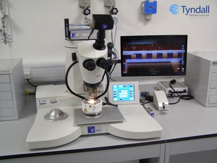
– Gold wire bonding (variety of wire sizes from 17µm to 50µm)
– Gold ribbon bonding.
– Gold stud bumping (for flip-chip assembly).
– Copper wire bonding (25µm)
– Aluminium wire bonding (25µm)
– Flip-chip alignment & bonding
– PCB design & layout.
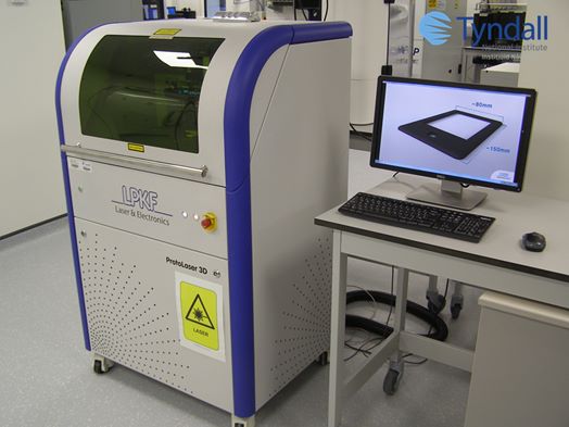
– 3D Prototyping for customised packaging solutions.
Technical specifications:
In all cases, Tyndall encourages users of its packaging capability to discuss their requirements in detail before committing to carry out any work. The will ensure the greatest likelihood of a successful outcome. Note that Tyndall’s packaging capabilities are suited to small (research-scale) volumes only (typically 10 to 20 units at most).
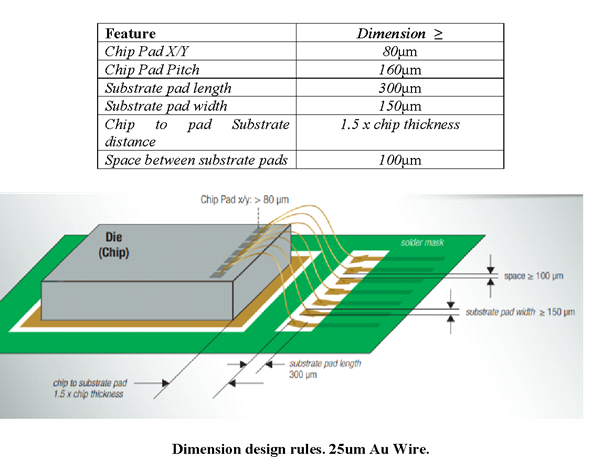
For all packaging tasks, the layout, geometry and metal finishes on both the die and substrate are of very high importance. Tyndall has prepared a detailed set of design rules which can be downloaded from the following web page: https://www.tyndall.ie/micro-electronics-micro-systems-packaging
As an example, the design rules for one of the more commonly used processes (25µm Gold wire bonding) are as follows:
Case study:
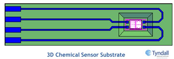
Development of a Low-cost 3D Chemical Sensor Package
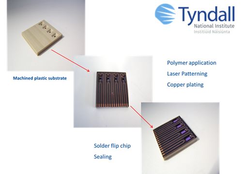
In this task, it was required to develop a low-cost packaging solution for a chemical sensor. The package was required to have a recessed area for the sensor chip such that a small quantity of liquid could be placed and retained on the sensor surface. The package was also required to protect the interconnect to the chip while the liquid sensing was in progress and be of a low cost, easily-manufactured design.
The solution developed by Tyndall was a customised package based on a machined plastic substrate onto which circuit tracks were patterned using the Tyndall LPKF Protolaser 3D system. Details of the process and images of the packaging solution are given below.
Process Summary
The process involved the following steps:
– Fabrication of a substrate with recess for sensor chip (machined from PEEK)
– Application of polymer coating containing metal particles (doped polymer).
– Design & layout of the circuit tracks.
– Patterning of track pattern on the polymer using the laser system (exposing the metal particles).
– Plating of a copper layer onto the patterned tracks.
– Plating of nickel / gold layers onto the copper tracks.
– Solder-based flip-chip attachment of the sensor chip.
– Sealing to protect the interconnection between package and sensor chip.
Benefits to the Researcher / Customer
– Customised packaging solution which enabled test & characterisation of sensor devices.
– Fast turn-around, quick to design and build in small numbers.
– Low cost solution.
– Easy to scale up & transfer to larger volume manufacture, if required.
Access Provider / Facilities