Etching Processes
About
The INL Cleanroom offers a comprehensive set of equipment for etching silicon, metal and dielectric layers.
Description
The INL Cleanroom offers a comprehensive set of equipment for etching silicon, metal and dielectric layers:
– The Deep Si etch is using the Bosch Process and can perform anisotropic etching of Si trenches with high aspect ratios and through-wafer vias.
– The Metal etch process includes Al etching, TiW, TiN and Al2O3 layers. It is capable of etching deep sub-micron features with near vertical sidewalls and provides good selectivity over the corresponding stopping layers and masks.
– The Dielectric etch process includes SiO2 etching but also etches SiNx and Al2O3 layers. It is specifically designed for “physical etch” processes of hard materials and is capable of etching deep sub-micron features with near vertical sidewalls and provides good selectivity over the corresponding stopping layers and masks.
– The Isotropic Si etch process exhibits nearly infinite selectivity of silicon to photoresist, silicon dioxide, silicon nitride and aluminum. As a vapor-phase etchant, XeF2 avoids many of the problems typically associated with wet processes. Accordingly, it is particularly well suited to MEMS applications.
– The Isotropic etch of sacrificial silicon oxide layers process uses HF vapor and alcohol vapor at reduced pressure and elevated temperature, providing a wide, stable process window that can etch different oxide compositions and thicknesses, while maintaining high selectivity to other common materials. Because of its dry nature, this process avoids stiction of released moving parts and damage to delicate structures.
– The Ashing process used to strip photoresist shows a good selectivity of resist with respect to metals and oxides and is a damage-free process for most materials, except the ones that deteriorate easily when exposed to oxygen (e.g., Ag, Cu, Cr, Fe, Ru).
Technical specifications:
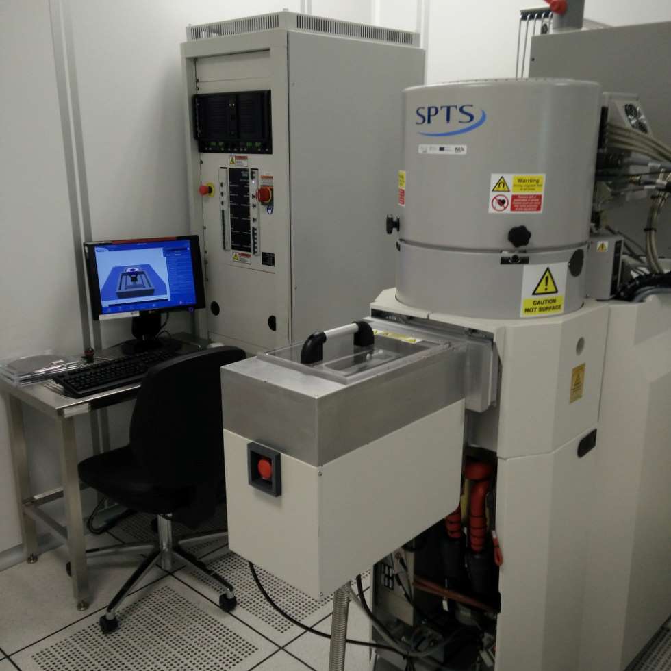
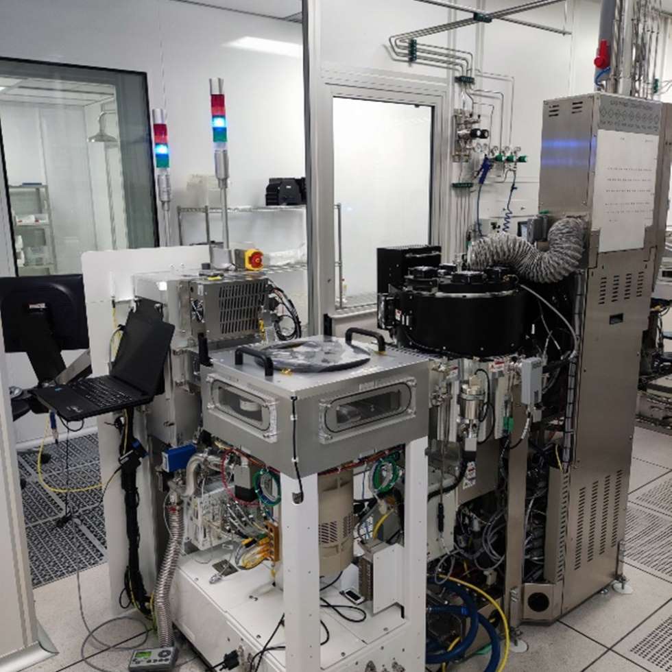
– SPTS Pegasus is a system dedicated for deep reactive ion etching of silicon using the Bosch Process. It uses a switched process by alternated cycles of SF6 plasma etching and C4F8 plasma for polymeric deposition. Helium gas is used for aiding backside cooling of the substrate.
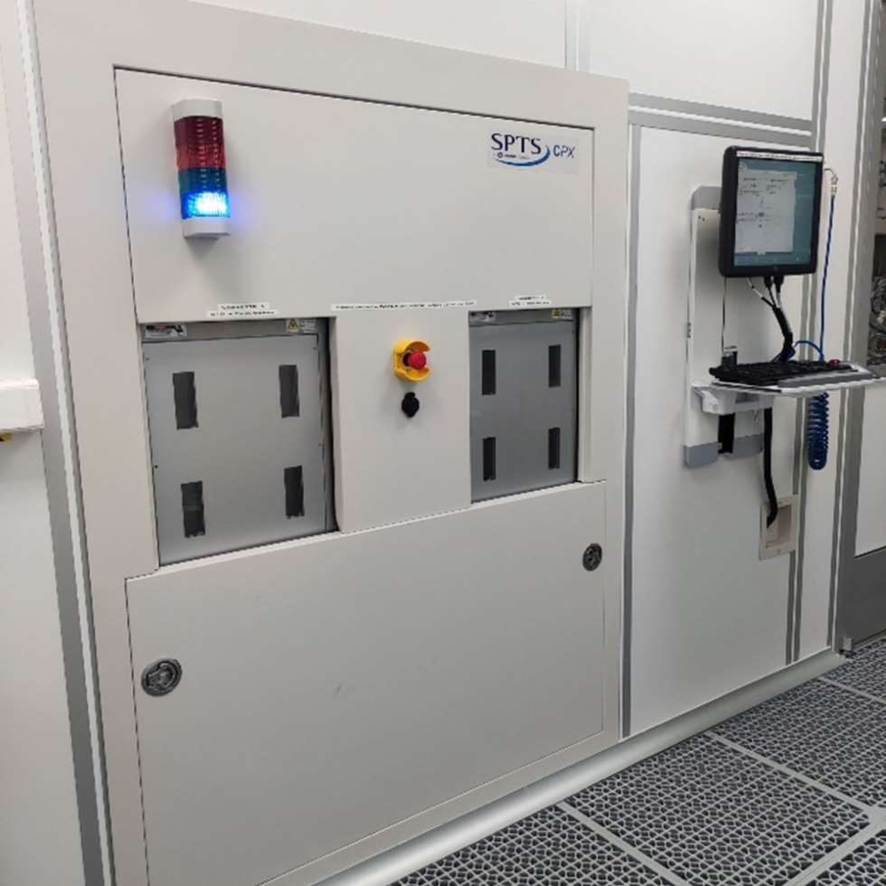
— SPST CPX Cluster system with dual loadlock and transport robot capable of batch processing of up to 50 200-mm wafers with 3 modules: a mixture of etch and deposition process chambers, for ultimate throughput and productivity, with possibility to perform sequential processes without breaking the vacuum:
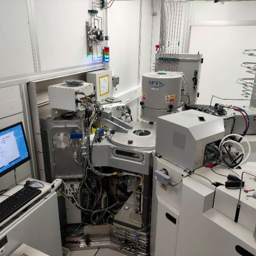
– SPTS APS Module is configured for etching of dielectrics, mainly dedicated SiO2 etching but will also etches SiNx and Al2O3 layers. It is specially designed for “physical etch” processes of hard materials.
– SPTS ICP Module is dedicated for Al etching but will also etches TiW, TiN and Al2O3 layers
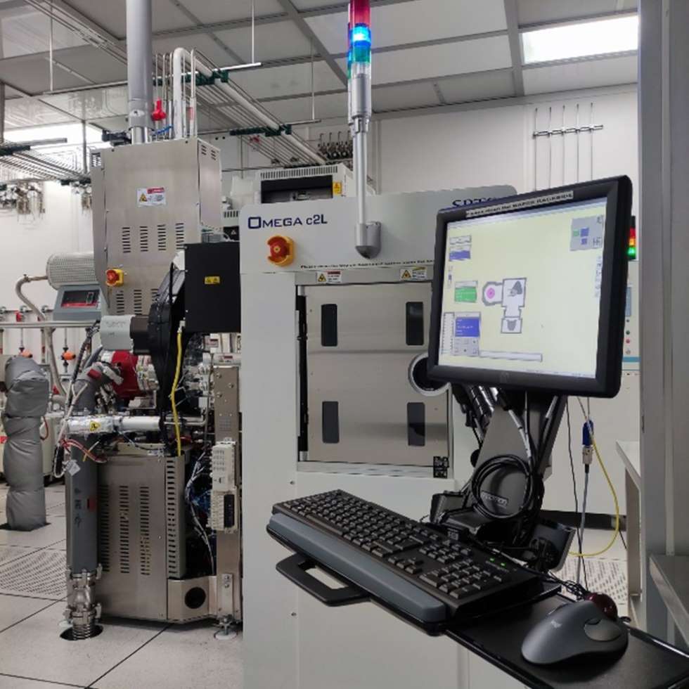
– SPTS c2L Omega ICP is a system dedicated for Al etching but will also etches TiWN, and Al2O3 and SiO2 layers. Helium gas is used for aiding backside cooling of the substrate.
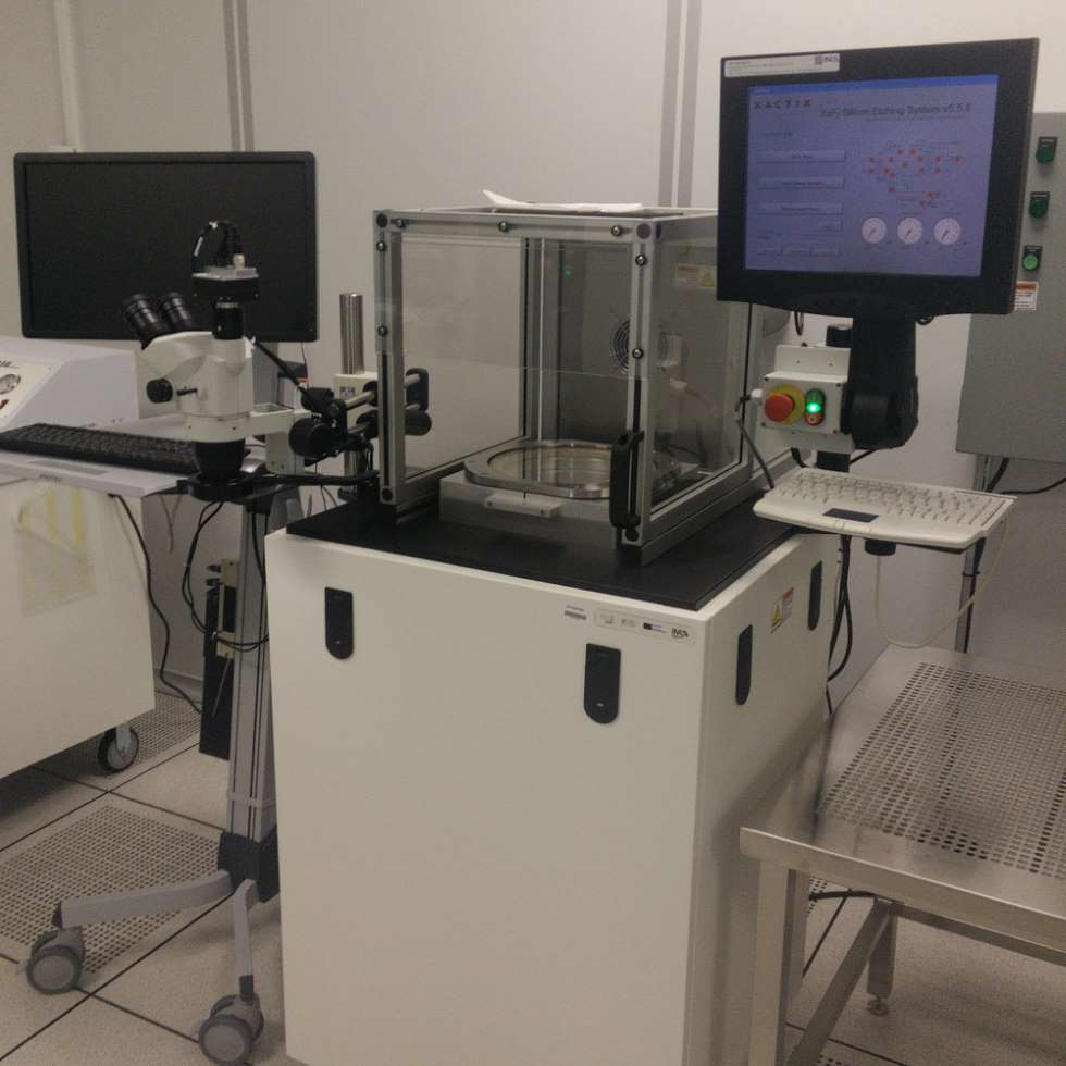
– SPTS Xactix X4 system is used for isotropic etching of silicon. The etch rates and uniformity are dtrongly dependent on the amount of exposed silicon, typically in the microns/minute range.
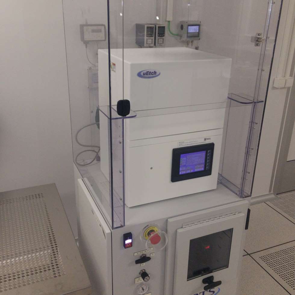
– SPTS Primaxx system is designed to isotropically etch sacrificial silicon oxide layers by combining anhydrous HF vapor and alcohol vapor at reduced pressure and elevated temperature.
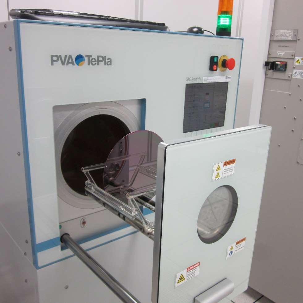
– PVA Tepla Plasma Asher is a system mainly used for photoresist stripping using a microwave plasma operating at 2.45 GHz with typical process pressures from 0.2 to 2 mbar. Other possible applications for this system are: surface cleaning before subsequent processes, descum after lithography, removal of organic passivating layers and masks.
Access Provider / Facilities