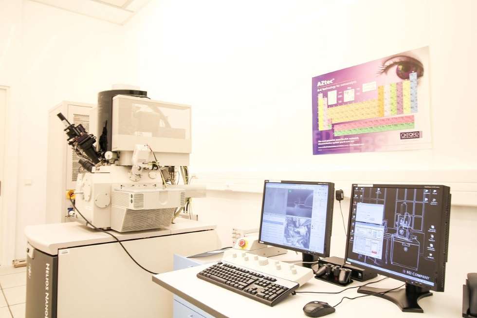
FIB-SEM System
About
A tool that combines a Scanning Electron Microscope (SEM) and a Focused Ion Beam (FIB) capability for sub-10-nm fabrication/patterning and materials analysis. A precise tool for real-time maskless micro-/nano-fabrication or for preparing TEM samples.
Description
Helios NanoLab 450S Dual Beam system is a highly versatile tool that combines SEM with FIB of gallium ions. The SEM operates with a field emission gun (FEG) that provides high beam intensity and stability. Imaging can be done with secondary (for SEM and FIB) and backscattered (for SEM) electrons. A STEM detector delivers resolution of 0.8 nm at 30 kV. For element analysis and mapping an EDX detector is available. An ultra-high resolution (UHR) stage and flip (for TEM lamella preparation) stages are available inside the microscope.
Technical specifications:
- Voltage (e-/i+): 0.5–30 kV
- HRSEM Imaging (Resolution 0.9 nm)
∙ Detectors: ETD, TLD, BSD, STEM (segmented – BF, DF and HAADF)
- EDX (Chemical analysis)
- FIB – Ga+ ions (Imaging/Patterning)
- TEM Lamella preparation
- Cross-section analysis
- Slice & View (3D reconstruction)
- Patterning: Milling/Deposition (Pt or W)
- Enhanced etching (Iodine) and Selective Carbon Etching (MgSO4 · 7H2O)
∙ Ultra-high resolution (UHR) and flip stages are available inside the microscope
∙ Fast entry lock chamber
Case study:
A user needs a lamella sample to be prepared for TEM imaging, this system has the comprehensive set of capabilities required for performing this task.
A user needs to inspect the internal structure of a device or device component. This system enables destructive analysis by preparing an individual cross-section or a sequential series of cross-section (for Slice & View imaging and 3D reconstruction). High-performance SEM provides the necessary imaging and EDX capabilities.
Optional:
https://inl.int/wp-content/uploads/2024/01/INL_BROCHURES_AEMIS.pdf
Access Provider / Facilities