GFET fabrication for sensing application on chip and wafer scale
About
AMO offers the fabrication of graphene devices (GFETs) for sensor applications. Users can obtain customised graphene devices on chip-scale as well as on 6” or 8” wafers. Electrical characterization on wafer scale can be offered additionally.
Description
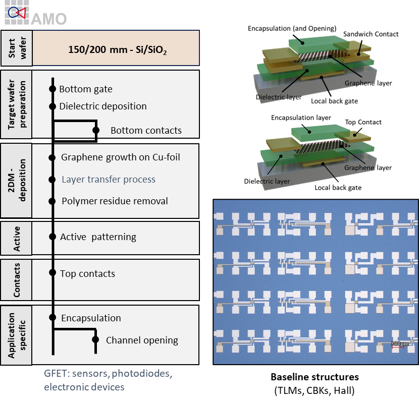
As a basis for an individual stack the existing process flow for encapsulated GFETs with backgate and different contact schemes can be used and can include the following steps:
- local /global back gate
- Dielectric deposition and via etching of the back gate pad
- Fabrication of adhesion pads
- Wafer-scale graphene transfer and pattering
- Contact fabrication
- Encapsulation and via etching on the contact pads
Furthermore, a device library is available with a Hall bar, a TLM structure device, a four-point measurement bar and a graphene sensing device that might be used e.g. as biosensor. For these devices, different dimensions are available and can be used as a basis for further modifications.
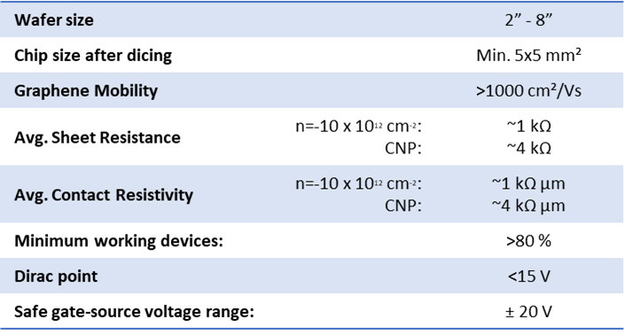
Electrical characterization on wafer-scale can be offered additionally.
Technical specifications:
Access Provider / Facilities