Maskless Laser Lithography
About
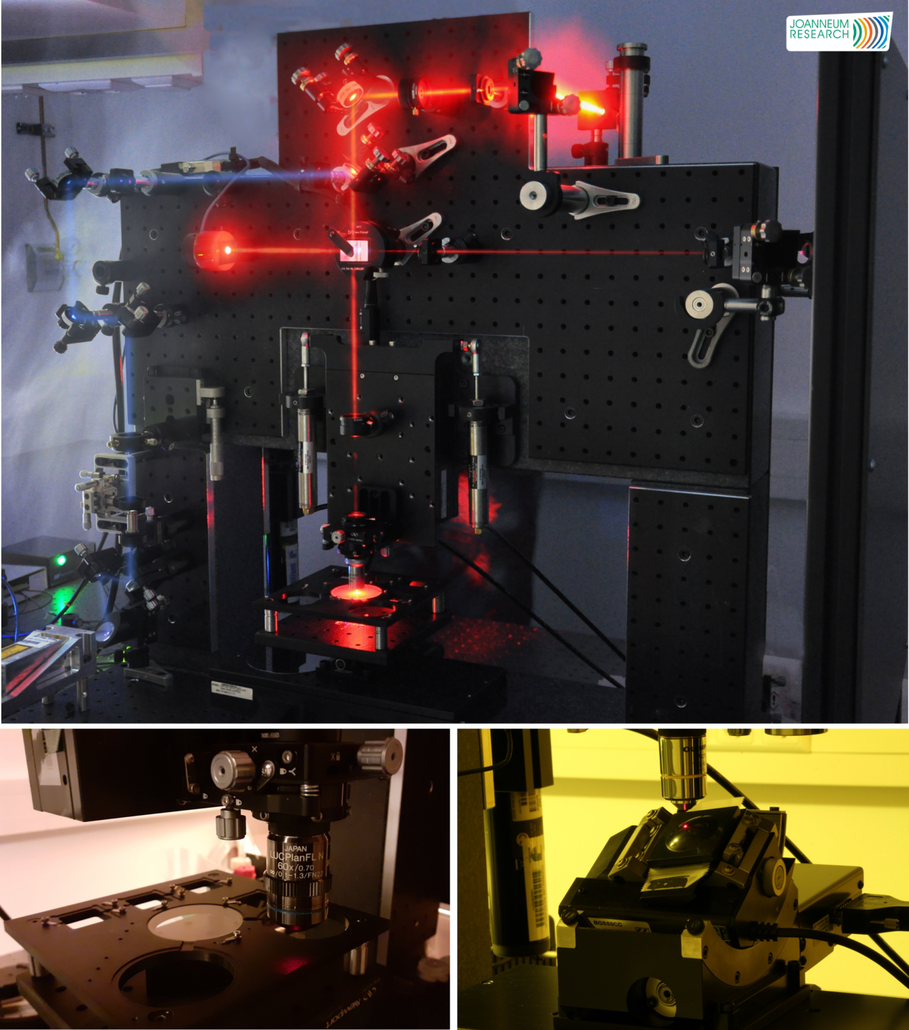
Maskless laser lithography system for creating high quality 1D, 2D and 2.5D microstructures
Description
With the maskless laser lithography (MALA) system we create high quality 1D, 2D and continuous-relief (2.5D) (sub-) microstructures on up to 6″ Si substrates. The lithography process is serial and resembles “optical milling”. First the Si sample is coated with a positive-tone greyscale photoresist layer of well-defined thickness. Then it is loaded on a high precision xy-stage and scanned under a focused laser diode. The writing parameters (e.g. illumination dose) for the laser are defined in a virtual photomask that was derived from the 3D model of the structure. The final step is the development of the patterned resist layer resulting in a removal of non-illuminated regions and the appearance of the relief structures.
Our patented technology also allows to fabricate 1-2.5D (sub)micron structures directly on 3D macro (planar and curved) objects to obtain new effects and functionalities.
Applications of MALA can be found in mastering for key enabling replication technologies like nanoimprinting or injection moulding and in rapid prototyping for photonics, optics, microelectronics and lab-on chip.
Technical specifications:
Specifications:
- Critical dimension
in XY: 200 nm, in Z: 120 nm - Maximal structure height: 60 µm
- Aspect ratio: 1:4
- Structure type: 1D, 2D, 2.5D and free-form
- Patterning on planar and curved substrates
- Laser writing speed of about 1cm2/h, depending on structure
- Integrated one-photon lithography (1PL), two-photon lithography (2PL) for creating 3D structures
- Laser wavelengths of 405 nm for 1PL and 780 nm for 2PL
- Maximum area of planar substrates: 16´16 cm2
- Maximum size of 3D macro-object with curved surfaces: 5´5´5 cm3
Link for additional information:
https://www.joanneum.at/materials/Infrastruktur/graustufenlithographie/
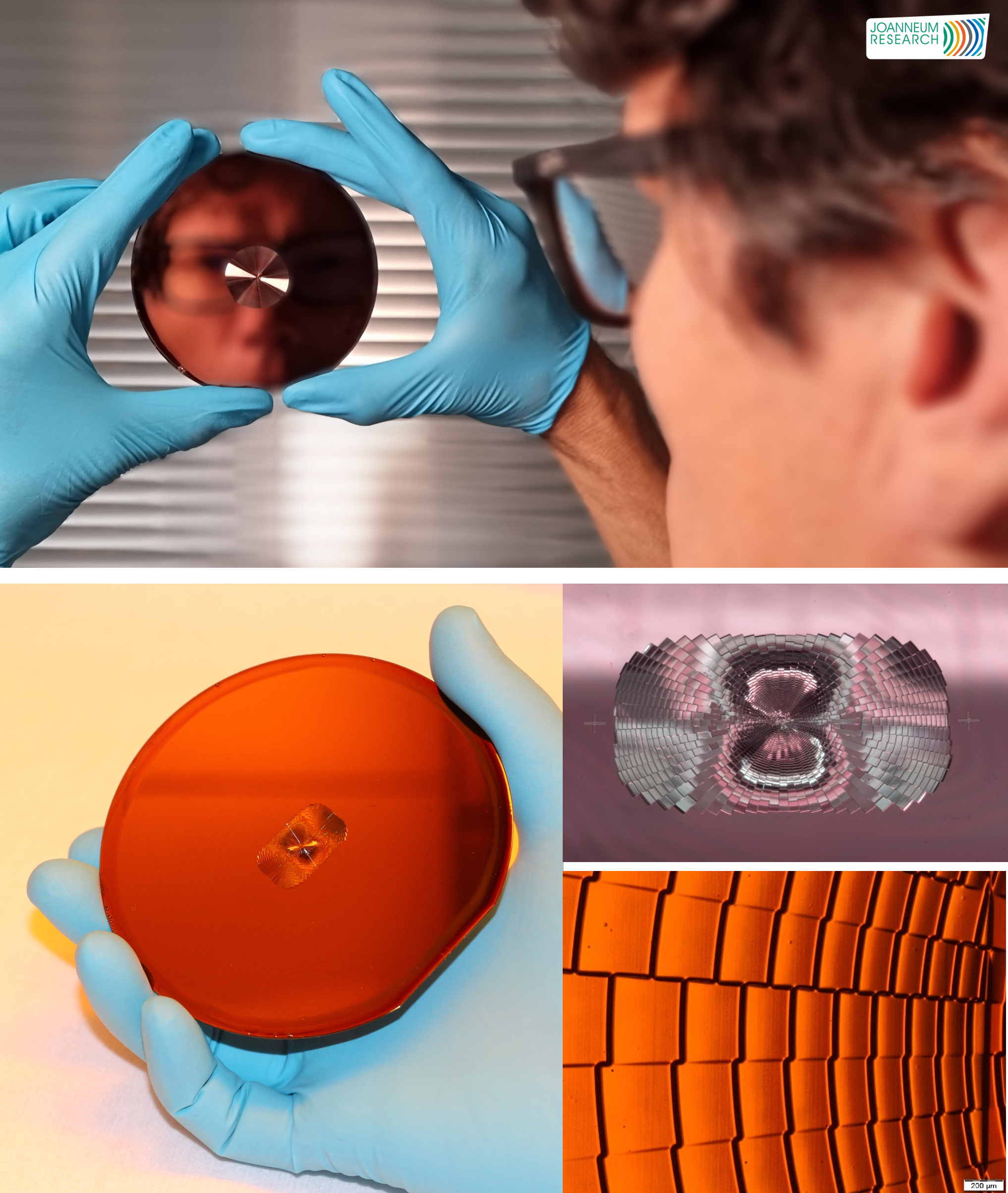
Case study:
A medical company needs a square submicron lattice surrounded by micro pyramids. From the design of this hierarchical structure, we calculate the virtual photomask that defines the laser writing parameters. A 2” wafer is then coated with the resist and patterned. The user receives the Si wafer with the developed resist showing the desired relief of nano and microstructures.
If desired, we can organize the electroforming of the MALA master in Ni at a partner. This yields a robust and durable Ni master and can be done for both structure orientations.
Access Provider / Facilities