Quantum superconducting circuits

About
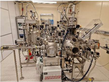
We offer a complete processing platform for fabrication of both low-Tc and high-Tc superconducting circuits for quantum technology applications. This includes growth of thin films by sputtering and electron beam evaporation, high-resolution electron beam lithography, plasma and reactive ion-beam dry etching, and advanced characterization of materials and devices.
Description
Chalmers offers a complete toolbox for fabrication of high-quality superconducting circuits based on both low- and high-critical temperature superconducting materials.
Key tools for the realization of the devices include:
– electron beam evaporation system with a high precision sample holder for shadow deposition of Al and oxygen gas inlet for fabrication of tunnel barriers.
– multiple sputtering tools for deposition of metallic superconductors (Nb, Al, NbTi, etc.).
– a cluster deposition system with pulsed laser deposition and oxide sputtering chambers for growth of YBCO superconducting films and multilayer structures.
– high-resolution nano-patterning using electron beam lithography.
– inert Ar+ ion beam milling with SIMS endpoint detection and liquid nitrogen cooling stage; dual-chamber ICP-RIE for chlorine- and fluorine-based processes.
Technical specifications:
Substrate materials and dimensions: Si/SiO2 or Al2O3 – typically 2” in diameter. Custom dimensions may be accommodated depending on the processing equipment.
Available materials examples:
Metals: Al (by evaporation), Nb, NbTi, Ti by sputtering.
Oxides: YBa2Cu3O7-x (PLD), SrTiO3 (RF magnetron sputtering).
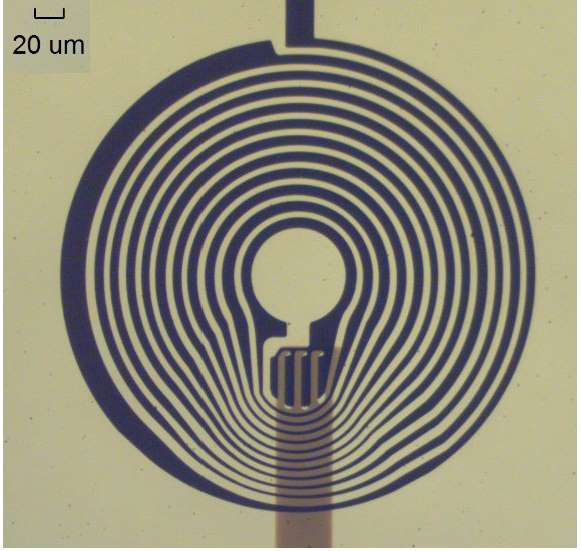
Patterning resolution: our electron beam lithography system is capable of making structures with linewidth of 10 nm and demonstrated alignment precision better than 10nm.
Access Provider / Facilities