Complex oxide electronics
About
We offer a complete platform for fabrication of complex perovskite-based oxide devices, including growth of thin films by pulsed laser deposition or sputtering, patterning using electron-beam lithography or direct laser writing, as well as ion beam etching using hard carbon masks. Wide range of materials is available for various applications, including ferroelectric, ferromagnetic, multiferroic and other functional Perovskite oxide materials.
Description
Perovskite oxides are a new family of quantum materials with a rich spectrum of physical and electronic properties such as superconductivity, ferromagnetism, ferroelectricity, and multiferroicity. A common crystal structure opens new ways to tailor multifunctional properties on atomic scale beyond conventional semiconductors. Chalmers offer different materials and a general flow from growth to patterning and characterization.
Key tools for the realization of the devices include:
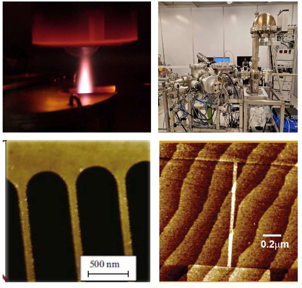
Fabrication:
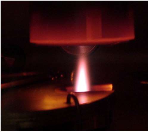
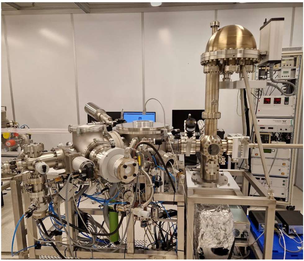
– Pulsed Laser Deposition systems with possibility of accommodating very different perovskite materials. One equipped with in-situ RHEED and XPS.
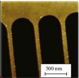
– High-resolution nano-patterning using electron beam lithography.
– Ar Ion beam milling using hard carbon masks.
Characterization:
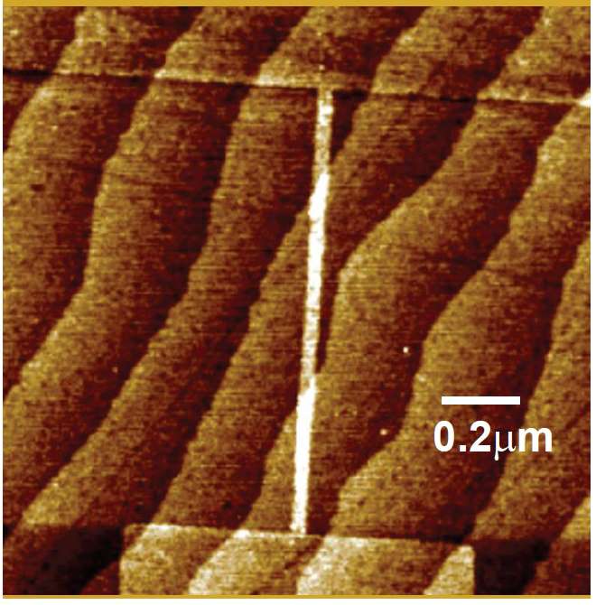
– High-resolution thin-film XRD for studying strain in thin films.
– State-of-the-art multimodal atomic force microscope for materials research.
Technical specifications:
The pulsed laser deposition systems are limited to a maximum substrate size of 10×10 mm2 and maximum deposition temperature of 850 °C for transparent oxides substrates. For oxide sputtering, thin films on larger wafers up to 2 inch in diameter can also be fabricated.
A very wide spectrum of oxide target materials is available for deposition. Chalmers readily offers established processing for standard oxides (YBCO, STO, LAO, LSMO, BTO). For non-standard materials, growth optimization upon changes in deposition parameters should be performed as a part of the offer package.
Reliable nano-patterning with resolution of < 50 nm can be achieved using EBL on insulating oxide materials. It is possible to fabricate structures with smaller dimensions, but the resolution will be most likely limited by the etching process.
We offer hard diamond-like carbon masks (DLC) fabricated by PLD for ion beam milling of hard oxide materials. Ion bean etching rate of DLC films is usually 10 times smaller than for most of oxides, which makes it possible to fabricate structures with very high aspect ratio.
Case study:
Prominent examples of devices that can be fabricated using this platform are:
– 2DEGs formed between LaAlO3/SrTiO3 with strong spin-orbit coupling for spintronic applications.
– Memristive systems for realization of new topological phases for quantum computing and neuromorphic networks.
Access Provider / Facilities