Tag Archive for: sputtering
 https://infrachip.eu/wp-content/uploads/2024/04/1_1_main.jpg
676
980
devinf20
https://infrachip.eu/wp-content/uploads/2024/01/infrachip-logo-3.png
devinf202024-10-17 09:06:292024-10-17 14:27:12Cleanroom Broad Fabrication Platform
https://infrachip.eu/wp-content/uploads/2024/04/1_1_main.jpg
676
980
devinf20
https://infrachip.eu/wp-content/uploads/2024/01/infrachip-logo-3.png
devinf202024-10-17 09:06:292024-10-17 14:27:12Cleanroom Broad Fabrication Platform
 https://infrachip.eu/wp-content/uploads/2025/02/CNRS_Spintec.png
429
949
Lina Jarboui
https://infrachip.eu/wp-content/uploads/2024/01/infrachip-logo-3.png
Lina Jarboui2024-06-24 13:53:422025-02-24 14:23:01SPINfab
https://infrachip.eu/wp-content/uploads/2025/02/CNRS_Spintec.png
429
949
Lina Jarboui
https://infrachip.eu/wp-content/uploads/2024/01/infrachip-logo-3.png
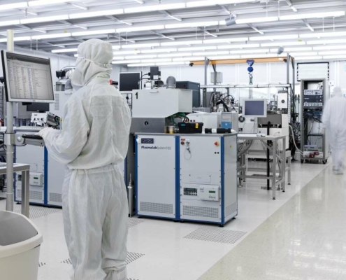
Lina Jarboui2024-06-24 13:53:422025-02-24 14:23:01SPINfab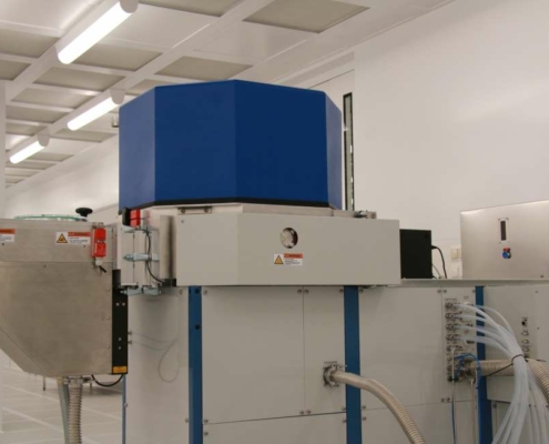 https://infrachip.eu/wp-content/uploads/2024/04/CEZAMAT_3-thin_film_depo.jpg
653
980
devinf20
https://infrachip.eu/wp-content/uploads/2024/01/infrachip-logo-3.png
devinf202024-04-12 14:16:422024-04-15 13:09:24Thin film deposition
https://infrachip.eu/wp-content/uploads/2024/04/CEZAMAT_3-thin_film_depo.jpg
653
980
devinf20
https://infrachip.eu/wp-content/uploads/2024/01/infrachip-logo-3.png
devinf202024-04-12 14:16:422024-04-15 13:09:24Thin film deposition