Cleanroom Broad Fabrication Platform
About
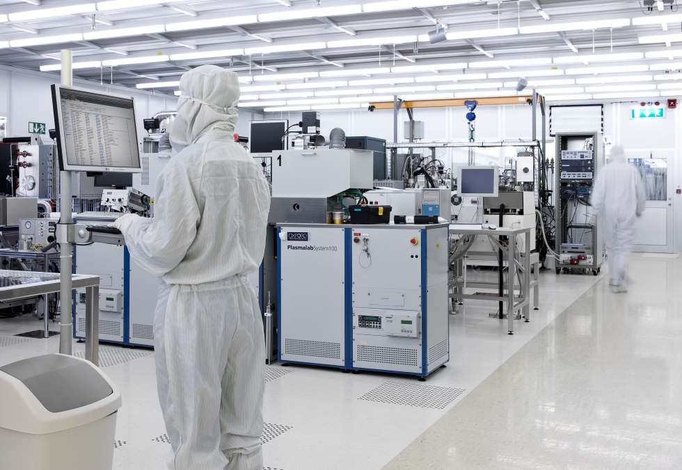
Myfab Chalmers offers a range of cleanrooms processes for full micro/nanofabrication. Deposition, etching, and lithography tools are available for a large range of materials and can be adapted for specific applications.
Description
The methods supported by cleanroom include:
– Deposition of metal and oxide materials (evaporation/sputtering/CVD depositions)
– Etching of several materials with high anisotropy with ready-to-use recipes
– Optical and e-beam lithography
– Processing of unconventional materials (2D materials, non-CMOS compatible)
– Fabrication of THz and RF devices
– High power devices
Technical specifications:
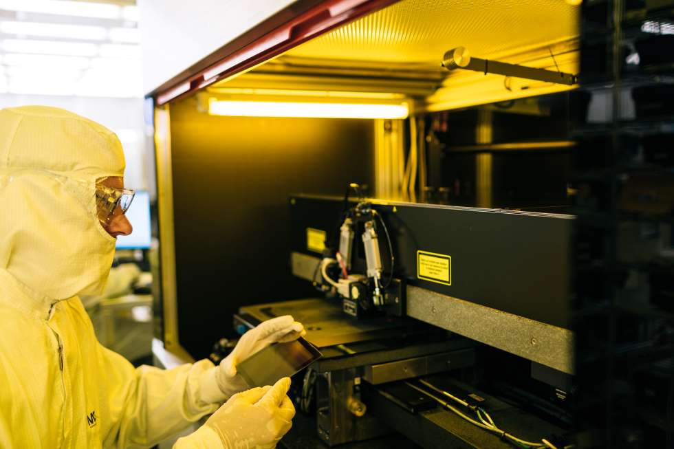
Lithography
- E-beam lithography: Raith EBPG 5200. High-resolution electron beam lithography system. 5mm to 200mm wafers. Interferometric stage and automatic height measurement system. Multicassette autoloader system. Minimum features size achieved: 8nm (HSQ). Alignment precsion: better than 10nm
- Direct Laser writer lithography: Heidelberg MLA150 (maskless aligner). Source: 375nm with output power of 6.4W. 5mm to 200mm wafers. High throughput tool. Minimum feature size: 1um. Front and backside alignment. Positive and negative resists (including SU8) available. Alignment precision: better than 250nm.
- Mask aligner: Suss MA/BA 6 mask aligners. Broadband emission. Back-side alignment available.
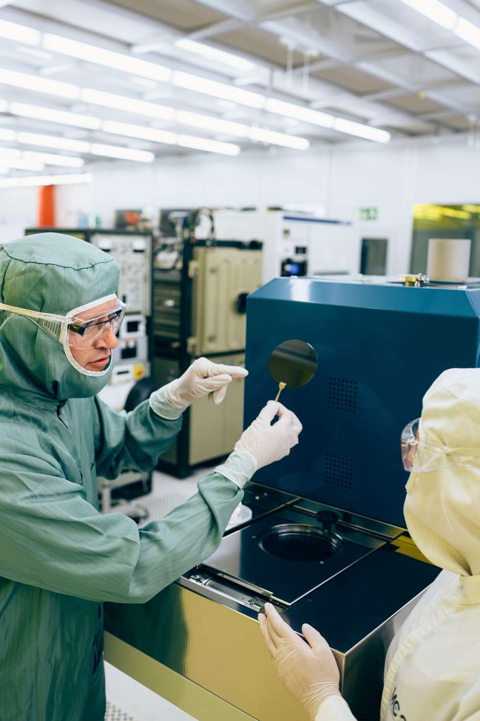
Deposition
– e-beam evaporation
- Kurt Lesker Flexible evaporator: metals and oxides. 5mm pieces to 160mm wafers. Sample tilt and rotation available.
– Sputtering
- FHR MS 150 Sputter: diverse metal, oxides and nitrides of high quality, low roughness. 5mm pieces to 150mm wafers. Substrate cooling and heating.
-CVD
- Oxford PECVD PlasmaPro 100. PECVD of silicon nitride and silicon dioxide for photonics, dielectric layers, passivation, and other uses. 5mm pieces to 150mm wafers.
- Centrotherm low-pressure chemical vapor deposition (LPCVD) tube furnaces. Deposition of stochiometric Si3N4 and low stress Si-rich SiNx. Deposition of a-Si and poly-Si. Deposition of TEOS. 5mm to 150mm wafers.
- Oxford FlexAl atomic layer deposition (ALD). Conformal thin deposition of following materials: Al2O3, AlN, HfO2, SiO2, Ta2O5. 5mm to 150mm wafer.
Etching
-Physical etching
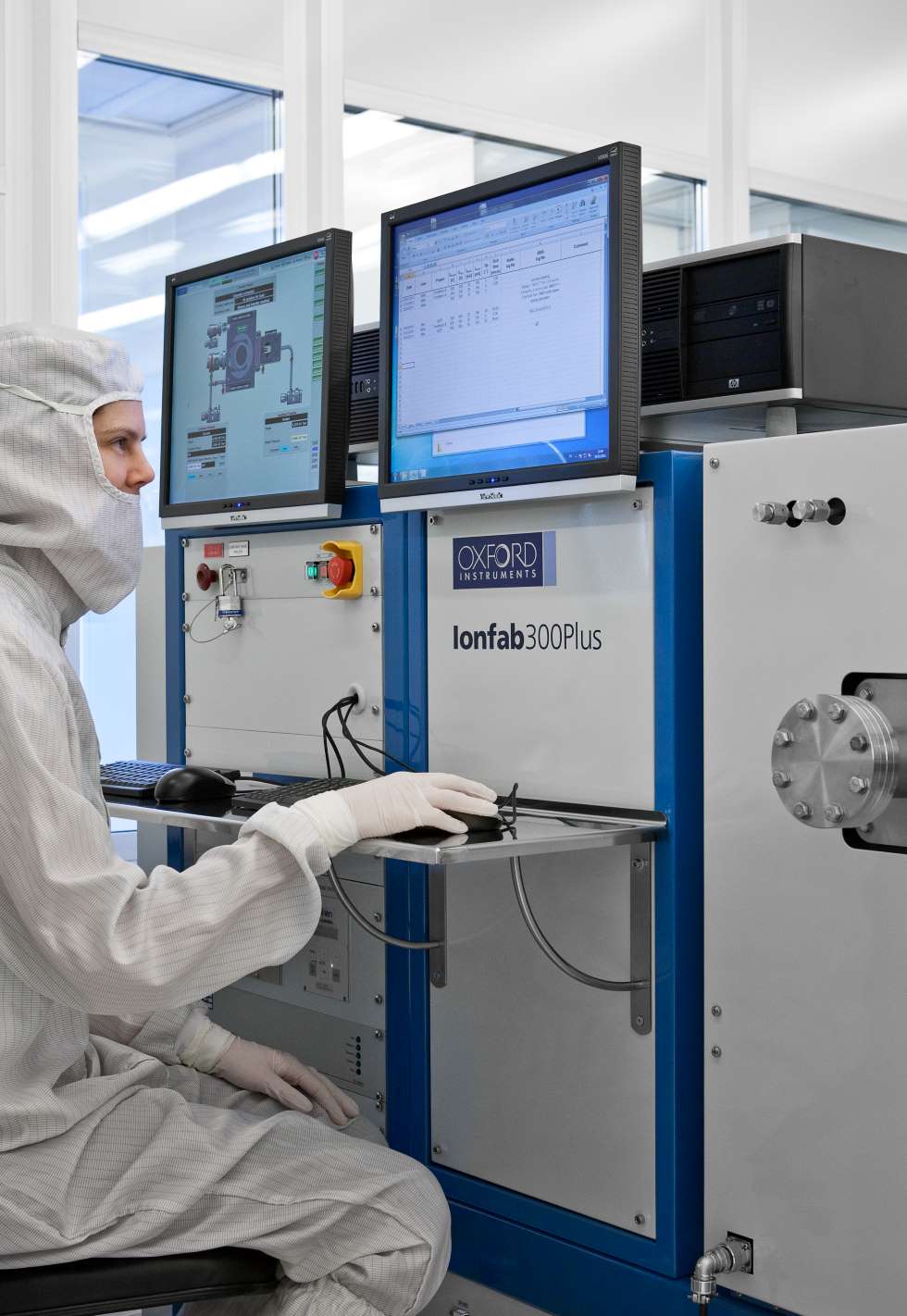
- Oxford Ionfab 300 Plus Ion Beam System. Inert Ar ion milling with SIMS endpoint detection. Etching using LN2 cooling available. 5mm to 100mm wafer.
- Oxford Ionfab 300 Reactive Ion Beam System for Chlorine based reactive ion-beam etching (RIBE). 5mm to 100mm wafer.
-ICP-RIE
- Oxford PlasmaPro 100 cluster. Double chamber ICP-RIE etching tool with separated Cl-based and F-based etching chemistry. 5mm to 100mm wafers. End-point detection.
- STS ICP-RIE dry etcher. HBr, Cl and SF6 etching gases available. 5mm to 100mm wafers. High temperature stage for compound semiconductor etching. End-point detection.
- Oxford Estrella for deep Si etch (Bosch Process). 5mm to 150mm wafers. Electrostatic clamp and substrate temperature control.
-Vapor etching
- Memstar XeF2 vapor release etching allows dry isotropic etching of Si at μm/min etch rates. 5mm to 150mm wafer.
Access Provider / Facilities
Chalmers University


