High-power probe station
About
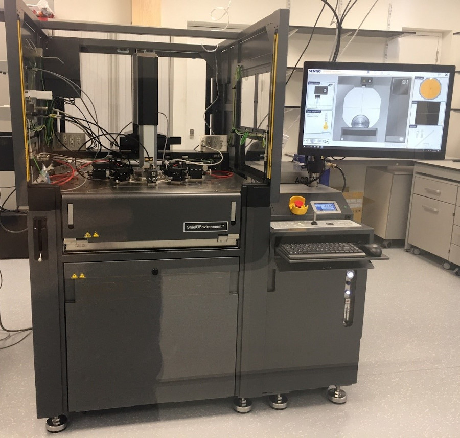
MPI High Power Semi-Automatic Probe Station (Model MPI TS3000 HP)
Description
300mm High Power Semi-Automatic Prober and High Power Parameter Analyser. For accurate and reliable high power measurements.
Dedicated design for high voltage and high current applications:
- On wafer high power measurement up to 10kV/600A
- Gold plated chuck surface for minimum contact resistance and vacuum holes optimised for thin wafers handling, down to 50μm
- Taiko wafer chuck option
- Dedicated high voltage and high current probes
- Anti-arcing solutions
Technical specifications:
Chuck: ∅300mm
Capability: up to 3000V (IV and CV)
Temperature range: -60°C to 300°C
MPI ShieldEnvironment for accurate measurements: Designed for advanced EMI/RFI/Light-tight shielding. fA low-leakage capabilities.
Ergonomic design and safety: Easy wafer or single DUT loading from the front. Regulatory approved safety interlocked light curtain to protect users. Integrated active vibration isolation. Completely integrated prober control for faster, safer and convenient system and test operation.
Safety Test Management (STM) option to load/unload wafers at any chuck temperatures and auto-dew point control.
Case study:
A researcher wants to investigate the effect of low T plasma treatment on Si nanowires (NWs). Using Tyndall test devices fabricated on SiO2-Si wafer in Tyndall. First they carry out comprehensive electrical characterisation of the devices during visit to the facility. Plasma treatment is then performed at the user’s. The treated devices are then electrically characterised again. The results show how the plasma treatment diffuses doping impurity from surface to bulk of the silicon NWs at low temperature and decrease the contact resistivity between metal contact and Si NW.
Optional:
High-power Probe Station (3D Virtual Tour)
Access Provider / Facilities