Lithography Processes

About
The INL Cleanroom offers a comprehensive set of equipment for flexible lithography process and product development, with an extensive portfolio of processes and photoresists.
Description
Optical and e-beam lithography processes with both positive and negative-tone resists are available for substrates from 200-mm-diameter wafers down to samples below 10 mm in size and square mask plates up to 9 inches.
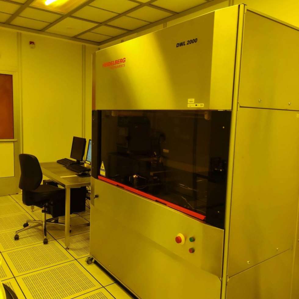
Direct-write lithography with a 405 nm laser writer for processing samples from 10 mm in size to wafers up to 200 mm and mask plates up to 9 inches, as well as exposure on flexible substrates.
With positive tone photoresists (AZ series):
- standard process thickness 600 nm, 1000 nm, 1200 nm, 2200 nm for wet and dry etch processes
- limited capabilities with 200 nm for highest resolution
- limited capabilities with 4 µm to 20 µm
- standard process with underlying LOR layer for lift-off process
- process with negative profile with 600 nm photoresist (for lift-off of metal deposition)
- bilayer resist with lift-off resist
- grey-level lithography (60 levels available) for 2.5D fabricated structures
With positive tone photoresist series for greyscale lithography (ma-P 1200 series):
- film thickness up to 60 µm
- grey-level lithography (128 levels available)
With negative tone photoresists (mr series):
- processes with 1 to 40 µm epoxy resin for direct-write for specific applications (microelectronics passivation, epoxy micromachines, microfluidics)
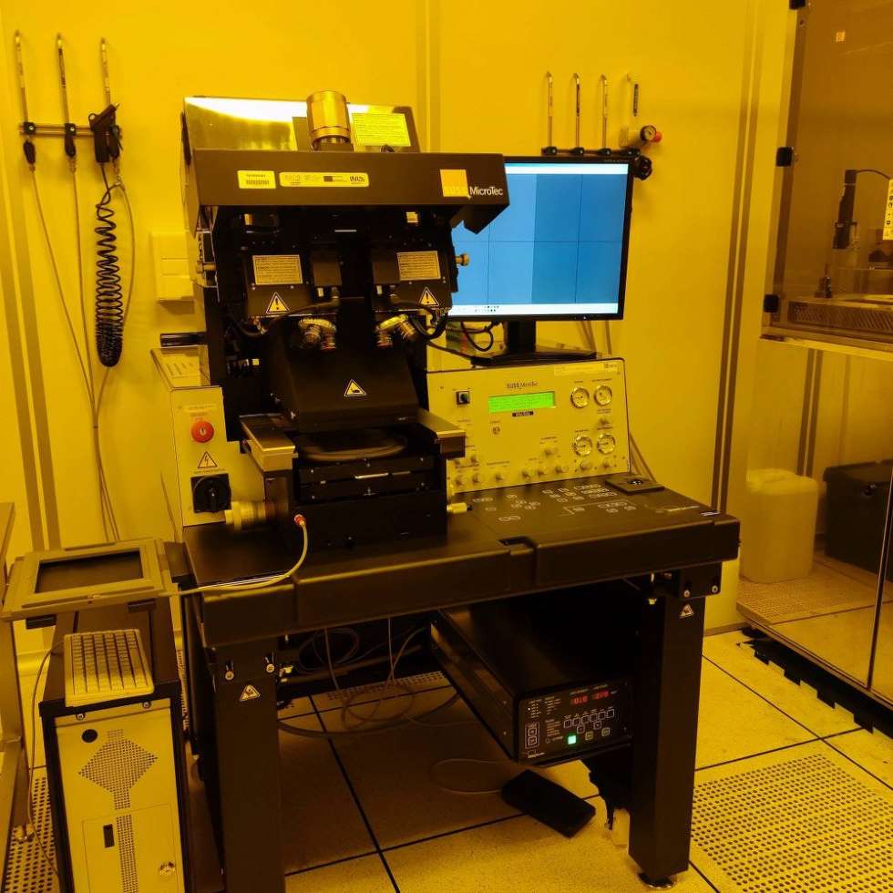
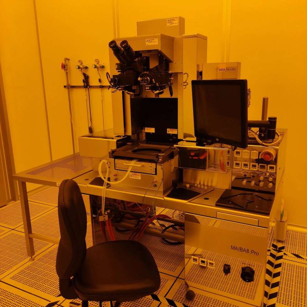
INL cleanroom is equipped two Mask Aligners dedicated for production. One uses a mercury lamp and 7-inch masks, using different UV bands with top and bottom alignment. The other uses 9-inch masks and an LED source; can perform automated alignments for an increased throughput and precision in aligned exposure from both top and bottom sides.
With positive tone photoresists (AZ series):
- standard process thickness 600 nm, 1000 nm, 1200 nm, 2200 nm for wet and dry etch processes
- standard process with underlying LOR layer for lift-off process
With special resists:
- UV-sensitive polyimide (e.g., for flexible devices)
- Photo sensitive ProTEK PSB (negative-working etch mask for KOH wet etch for silicon micromachining)
- UV-sensitive SU-8 (negative tone photoresist up to 150 um thickness)
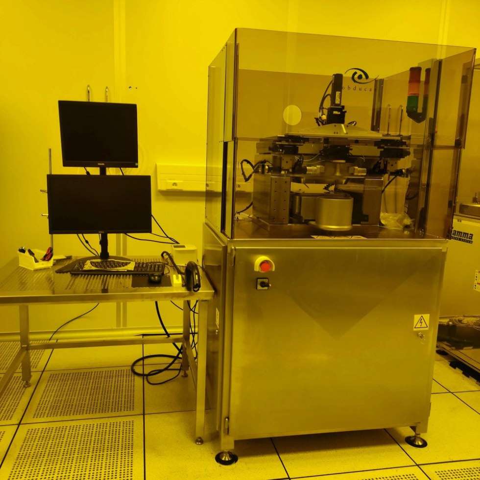
Nanoimprint lithography is a recent addition to the capabilities of INL, enabling the patterning of a wide range of hard and soft materials and the fast fabrication of 3D micro- and nanostructures in a single step. The masters to be used for imprint can be produced using our DWL or EBL tools.
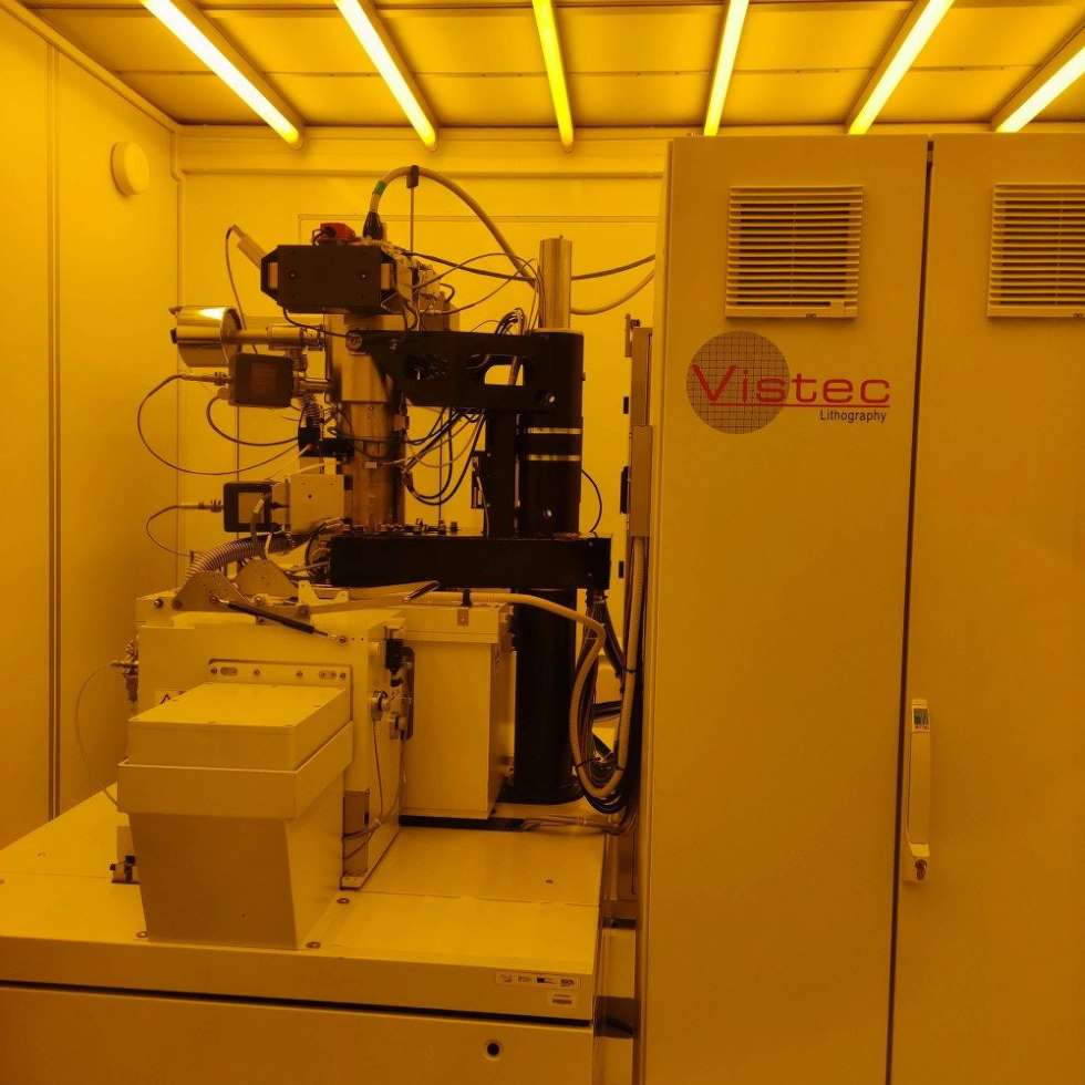
INL is equipped with e-beam lithography which has demonstrated resolution down to 7 nm.
A range of photoresist options has been validated
- positive tone PMMA 100 nm to 430 nm and bilayer PMMA processes for lift-off of nanostructures
- positive photoresists ZEP520 and AR-P 6200 for etching applications
- negative tone AR-N 7520 for etching of nanopillars, range 80 nm to 800 nm in thickness, achieving typically 50 nm lateral size for 200 nm photoresist thickness.
- Limited testing on HSQ negative tone resist for highest resolution and semiconductor applications
- Epocor/Epoclad epoxy resist for direct write of optical waveguides
The e-beam system accepts wafers of 3 inch and 200 mm in diameter, sample parts of irregular shapes fitting into a 76 mm circular holder, and glass masks 6 inch in diameter.
The e-beam exposure files are converted using Genisys Layout Beamer and can include proximity effect correction in dose factor and in shape
Technical specifications:
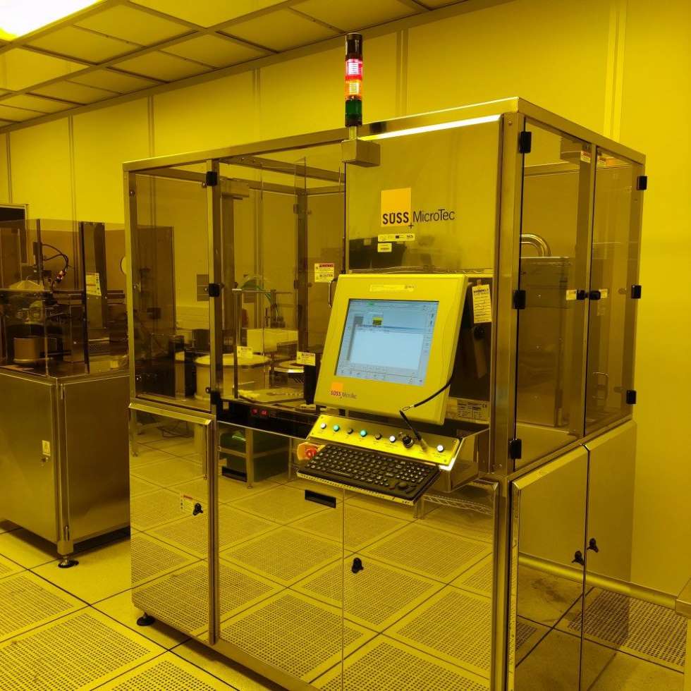
— Suss Microtec: High-throughput Coating & Development Process.
– Handling of round and square substrates up to 200mm.
– Thin, thick resists, polyimide.
– Precision edge bead removal.
– Process up to 25 wafers in one batch.
— Suss Microtec: Optical Exposure with Mask Aligner.
– Substrates up to 200 mm.
– Masks from 2″ to 9″ plates.
– Broadband wavelength: 365/405 nm.
– Modes of operation: Soft, Hard and Vacuum Contact, Proximity exposure and Flood exposure
– Automatic alignment and backside-alignment capability.
— Heidelberg: Exposure with Direct Write Laser.
– Substrates up to 200 mm.
– Minimum structure size: 700 nm.
– Autofocus: optically or pneumatically.
– Auto-measurement capability.
– Grey-level lithography with 128 levels.
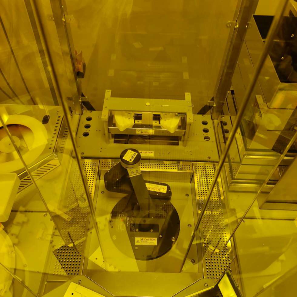
— Obducat Eitre 8: Nanoimprint lithography system.
– Allows both thermal and UV nanoimprint lithography.
– Full area: 8-inch square.
— Vistec E-beam Lithography
– Thermal Field Emission gun for operation at 50 and 100 kV and up to 100 nA beam current.
– Capability of writing on Si and other substrates (glass, metals, SiO2,) up to 200 mm size.
– Capability of writing 150-mm optical masks for contact and projection lithography.
– Write field up to 520 µm.
Access Provider / Facilities