Transmission Electron Microscopy
About
Three (Scanning) Transmission Electron Microscopes are available at INL, with a wide range of capabilities for imaging, crystallographic analysis, and elemental mapping.
Description
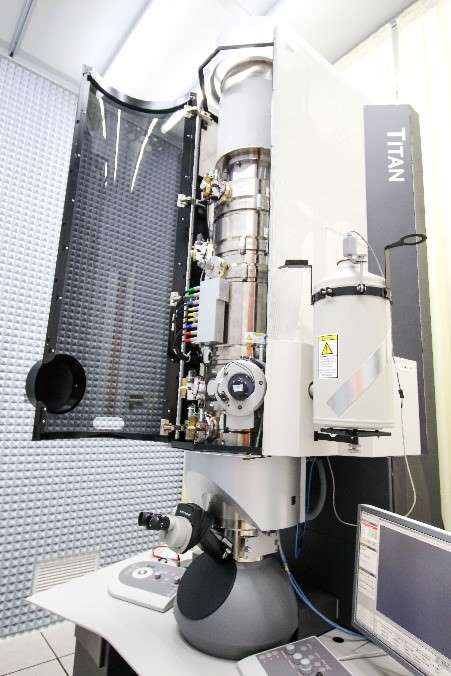
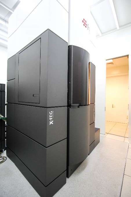
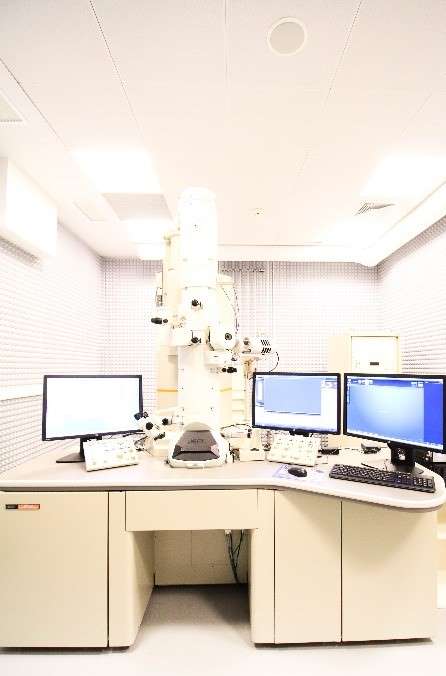
The three (Scanning) Transmission Electron Microscopes [(S)TEM] offer access to a range of techniques. The JEOL2100 is optimized for TEM imaging of large areas, fitted with a fast-readout “OneView” 4k x 4k CCD camera that operates at 25 fps (300 fps with 512 x 512 pixels), as well as high-resolution imaging and crystallographic analysis. The Titan ChemiSTEM is a probe-corrected (S)TEM optimized for elemental analysis at low-to-high resolutions, fitted with four energy dispersive X-ray spectroscopy detectors and an electron energy loss spectroscopy (EELS) system. The microscope also carries out atomic-resolution imaging, with contrast from the atomic weight of the elements, in high-angle annular dark field. The Titan ChemiSTEM is also optimized for electron tomography for 3-dimensional reconstruction of materials. Finally, the Titan Themis is a double-corrected (S)TEM for high-resolution imaging and elemental analysis with sub-angstrom resolution in TEM and STEM, and a monochromator for chemical analysis.
Technical specifications:
Double Corrected TEM/STEM Titan Themis:
- Voltage: 60–300 kV (X-FEG)
- Monochromator
- Corrected TEM Imaging (Resolution 63 pm)
- Corrected STEM Imaging (Resolution 63 pm)
- Diffraction (Crystallographic analysis)
- EDX – Super X (Chemical analysis)
- Dual EELS (Energy resolution 190 meV)
- Electron Holography
- Lorentz microscopy
- In-situ sample holder (heating/biasing)
- Differential Phase contrast (DPC) imaging
Probe-corrected STEM Titan ChemiSTEM:
- Voltage: 80 – 200 kV (X-FEG)
- TEM Imaging
- Corrected STEM Imaging (Resolution 80 pm)
- Diffraction (Crystallographic analysis)
- EDX – Super X (Chemical analysis)
- EELS (Energy resolution 1 eV)
- TEM/STEM Tomography (3D Reconstruction)
JEOL2100:
- Voltage: 80 – 200 kV (LaB6)
- TEM Imaging (Point Resolution <230 pm)
- STEM Imaging
- Diffraction (Crystallographic analysis)
- Cryo (Biological samples/Soft matter)
- Tomography (3D reconstruction)
- EDXS (Chemical analysis)
Case study:
A user needs to carry out elemental and crystallographic analysis on lamella samples (less than 100 nm in thickness) prepared from devices (or materials/components). The typical applications of these techniques are for analysis of critical dimensions, defects, and failures in devices or materials, down to sub-nm scale.
Optional:
https://inl.int/wp-content/uploads/2024/01/INL_BROCHURES_AEMIS.pdf
Access Provider / Facilities