 Dear readers,
Thank you for your interest in INFRACHIP!
This is the 3rd Newsletter of the project, and we would like to update you on how things are progressing.
INFRACHIP focuses on addressing modern challenges in the field of semiconductors by helping researchers and companies to find ground-breaking solutions for novel chips. How? By providing a free and facilitated access to state-of-the-art facilities and technologies, thanks to funds from the European Union.
Since our last newsletter, we have significantly augmented our portfolio of offerings.
You can visit the showroom to discover additional technologies in sustainable solutions, sensors, powering, RF technologies, quantum/spin device engineering, NVM and much more. Be sure to take a look!
If you cannot find what you are looking for, you can always contact us to discuss your needs.
We are looking forward to starting projects with you and welcoming INFRACHIP users across various facilities.
In the past few months, we have been very excited to welcome more promising talents into our training programmes, through the Research Accelerator Programmes. You’ll find out more about that a bit later, so we’ll keep the suspense going until you move to the first item of this newsletter 😉
Moreover, we just concluded the first part of the very first INFRACHIP school (organised by HMU) on 2D Materials for Flexible Energy Harvesting and Storage Devices. We held a series of online talks with various speakers from a much larger network than INFRACHIP. This was a real success. We hope to organize many such events in collaboration with experts from leading universities and research centres, to share ideas and knowledge on key semiconductor related topics.
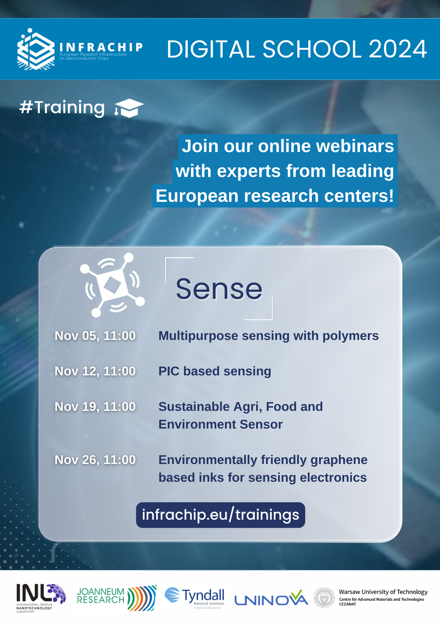
In the meantime, you can join our Digital School to learn more about sensing (and we will also divulge more in this newsletter)!
Enjoy reading this newsletter!
The INFRACHIP Team
![]()


 Dear readers,


