Photonic Integrated Circuits
About
Silicon nitride passive photonic integrated circuits operating in VIS and C-band for user-defined applications. Custom design comprises elements defined in a library of building blocks or user-defined within design rules.
Description
The use of photonic integrated circuits in sensing applications allows for the expansion of the application area of systems. Optical-based sensors exhibit higher long term-operation stability, sensitivity, selectivity, and short response time. These qualities make them applicable for real-time in situ applications like remote air quality monitoring, gas leak detection systems, bio-markers detection, and high-end market applications.
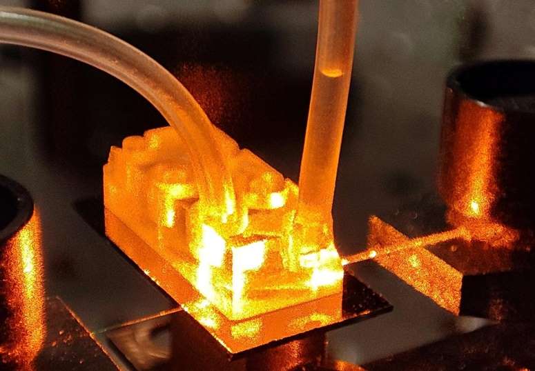
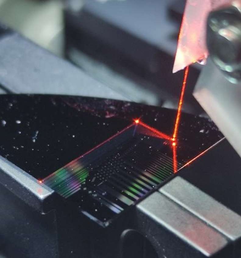
We offer expertise in the development of photonic integrated circuits (PICs) operating in visible and C bands. The main applications are biosensing and environmental sensing. However, we do not refrain from other fields. Our experience covers full development cycles: simulation and design on the element and circuit level, fabrication, and characterization.
Selected key equipment of the technology line are:
- Electron beam lithography tool for fabrication of nanometric scale patterns on substrate, used for fabrication of precise patterns as well as fabrication of photomasks
- Furnaces and Low Pressure Chemical Vapour Deposition for medium and high temperature) for annealing and oxidation and of silicon substrates as well as deposition of polysilicon and silicon nitride (SixNy) layers
- Dry etching system in chlorine or fluorine plasma enhanced by reactive ions with inductively coupled plasma
These are accompanied by: Rapid Thermal Processing (RTP) furnace, batch spray systems, Plasma Enhanced Chemical Vapour Deposition (PECVD) system, magnetron sputtering system, Semi-automatic resist processing system for mask cleaning and chemical processing on single wafers, mask aligner for photolithography wafer bonding system, spectroscopic ellipsometer with spectral range: 190nm – 2100nm for determining thickness and optical parameters of thin films, high resolution scanning electron microscope.
Technical specifications:
1) Wavelengths: 460 – 670 nm; 1500 – 1600 nm, Other wavelengths – custom development
3) SiN height: 120nm, 400nm, Other heights – custom development
5) Waveguides, bends, tapers, MMIs, AWGs, grating couplers, MZIs, RRs, Other elements –custom development
Case study:
A user would like to design the photonic integrated device and fabricate it for characterization. Fabricated elements can be optimized for sensing applications.
Optional:
Lelit, M.; Słowikowski, M.; Filipiak, M.; Juchniewicz, M.; Stonio, B.; Michalak, B.; Pavłov, K.; Myśliwiec, M.; Wiśniewski, P.; Kaźmierczak, A.; et al. Passive Photonic Integrated Circuits Elements Fabricated on a Silicon Nitride Platform. Materials 2022, 15, 1398. https://doi.org/10.3390/ma15041398
Access Provider / Facilities