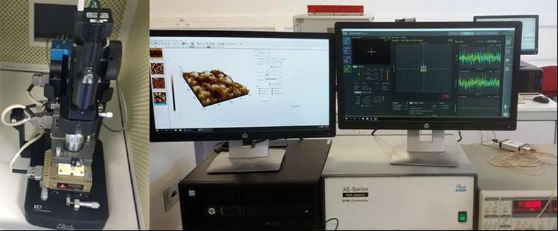
Park XE7 AFM platform
About
Atomic Force Microscopy (AFM) platform including Scanning Kelvin Probe Microscopy (SKPM), Dynamic Contact EFM (DC-EFM) and Piezoresponse Force Microscopy (PFM) modes
Description
Atomic Force Microscope system for small and medium size samples, consisting of completely decoupled XY & Z scanners using flexure guided scan system for all three axes, closed/open-loop scan, XY flexure scanner with zero background curvature, XE AFM head, direct on-axis optics, high resolution digital CCD camera with digital zoom, motorized Z stage, manual focus stage, precision manual XY sample stage, control electronics, computer, software and cantilevers.
Technical specifications:
- XY scanner with closed-loop feedback control
– Single module parallel-kinematics flexure stage
– Scan range: 50 × 50 μm
– Resolution: < 0.6 nm (closed-loop), < 0.01 nm (open-loop)
- Z scanner with closed-loop feedback control
– Guided flexure stage
– Scan range: 12 μm
– Noise level: 0.03 nm (typical) / 0.05 nm (maximum)
- Enhanced EFM, Scanning Kelvin Probe Microscopy (SKPM), Dynamic Contact EFM (DC-EFM) and Piezoresponse Force Microscopy (PFM) modes.
- Supports standard AFM/SPM modes including True Non-contact mode, dynamic contact mode, contact mode, LFM (lateral force microscopy), F/D spectroscopy, and phase imaging with no need of additional software/hardware option.
- Performs MFM, EFM, FMM, and Nanoindentation
Case study:
With the AFM system, the INFRACHIP user can analyze semiconductor materials and devices with unprecedented detail, providing insights into their structural and mechanical properties. This information is essential for optimizing device performance, identifying defects, and improving manufacturing processes. By leveraging the advanced capabilities of the AFM system, the user can conduct cutting-edge research in semiconductor materials and device engineering, contributing to advancements in semiconductor technology.
Access Provider / Facilities