Raytracing ASAP Breault Research

About
ASAP is a commercial raytracing software for simulating the behaviour of optical components or entire optical systems. This technique is based on the geometrical optical equations; therefore, the propagation of light is described in terms of rays, which are “traced” trough the simulation area. At suitable positions inside the optical system, the rays can be stopped and evaluated. Complemented by self-developed algorithms for calculation, design and optimization of optical components for tailored light management solutions.
Description
– Full geometrical control of surfaces inside the simulation area to build realistic models of the simulated optical models.
– Up to 100k different surfaces possible in one simulation model
-Very high simulation speed, depending on the complexity of the optical model several millions of rays can be traced in minutes.
-Different optical properties can be attached to the surfaces in the simulation model like e.g. a change of refractive index, reflecting/absorbing properties or scatter models.
-Realistic models of light sources or ray files measured by LED manufactured can be used for the simulations.
-Investigation and optimization of optical systems with regard to various optical properties, e.g. system efficiency, generated irradiance distributions at arbitrary positions, generated radiance distribution of the optical system.
-Evaluation of the stability of an optical system with regard to manufacturing and assembly tolerances by means of tolerance simulations
-Possible use of a portfolio of algorithms developed in-house over more than 10 years to develop tailor-made light management solutions achieved, for example, through the use of extremely flat (height <50 µm) free form micro optical elements
https://en.wikipedia.org/wiki/Geometrical_optics
Case study:
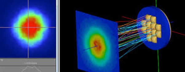
A user needs an optical system for optimizing the illumination of a direct-lit luminaire. With the software ASAP we can design optical structures that generate an irradiance distribution with a specified shape at the target plane. The design is based on a realistic model for the mounted LED array. The outcome is a 3D model of said optical structure, optionally with a freeform surface, that can then be manufactured in a material of the target refractive index either by the user or by the access provider with maskless laser lithography.
Optional:
Leiner, C., Nemitz, W., Schweitzer, S., Wenzl, F. P., & Sommer, C. (2020). Design procedure for ultra-thin free-form micro-optical elements allowing for large DHR values and uniform irradiance distributions of ultrathin direct-lit luminaires. OSA Continuum, 3(11), 3237-3252.
DOI: 10.1364/OSAC.404268
Zauner, M., Muehleisen, W., Holzmann, D., Baumgart, M., Oreski, G., Feldbacher, S., … & Reil, F. (2022). Light guidance film for bifacial photovoltaic modules. Renewable Energy, 181, 604-615.
DOI: 10.1016/j.renene.2021.09.069
Lichtenegger, F., Kröpfl, A., Leiner, C., Sommer, C., Krutzler, C., & Weiss, A. P. (2024). Privacy preserving image sensor based visible light positioning receiver utilizing an ultra-flat singlet lens with high field-of-view and high aperture. Optics Communications, 556, 130243.
DOI: 10.1016/j.optcom.2023.130243
Toren, P., Smolka, M., Haase, A., Palfinger, U., Nees, D., Ruttloff, S., … & Hesse, J. (2020). High-throughput roll-to-roll production of polymer biochips for multiplexed DNA detection in point-of-care diagnostics. Lab on a Chip, 20(22), 4106-4117.
DOI: 10.1039/D0LC00751J
Access Provider / Facilities