Test & Characterization Platform
About
Test and Characterisation Platform - Electrical, optical and physical characterization of materials and devices at multi-levels, supported by physics-based modelling
Description
– DC and quasi static electrical (I-V, C-V) characterization set-ups compatibles with various devices and platforms and various operating conditions (large range of temperatures, bias and mechanical stress, pressure-controlled probes, environmental control, magnetic field, light, very low current…). Physical modelling of semiconductor devices and extraction of electrical parameters (mobility interface states density, threshold voltage…)
– Spectroscopic techniques: defect spectroscopy (DLTS, admittance spectroscopy), pulsed and dynamic measurements, quantum efficiency (IQE, EQE), spectral response, reflectance spectroscopy (with integrating sphere), Second Harmonic Generation (SHG).
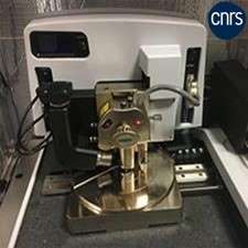
– Nanometric scale characterization: AFM (Atomic Force Microscopy) with tapping and contact topographic modes and various electrical modes including SMIM (Scanning Microwave Impedance Microscopy), PFM (Piezoresponse force Microscopy) and C-AFM (conductive atomic force microscopy).
Technical specifications:
– Semiconductor parameter analyzer Agilent B1500A supporting IV, CV, pulsed/dynamic IV measurements (10ns time response, current down to fA).
– Precision LCR meter Agilent 4980A, 20Hz-2MHz.
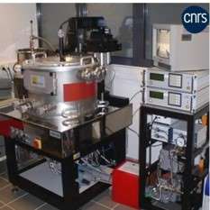
– PhysTech HERA-FT1030 system: (DLTS, PICTS, optical DLTS…): 10K-360K
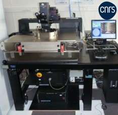
– Manual probe cryo-stations: 4 probes 200mm SuSS MIcrotech cryo-station (9K-330K); 50mm ambient controlled Microworld 4 probes station (77K-870K), 100mm 6 probes low noise Lakeshore closed loop helium station (6K-350K) (up to 40GHz)
– Automatic probe station: 300mm ELITE 300 (300K-380K)
– Janis cryostat for bounded samples on DIL holders (9K-380K, 0.9T magnetic field for Hall measurements)
– JANDEL pressure-controlled probes (pseudoMOS, very thin or sensitive layers)
-Xenon lamp, monochromator Oriel (two gratings covering a wavelength range of 300nm-1500nm), two photodetectors (Si, Ge)for EQE measurements. EGG lock-in amplifier, integrating sphere (with two detectors, two calibrated samples.)
– Femtometrix SHG system: incident femtosecond laser (780nm wavelength, power 10 mW- 120mW), 300mm wafer, mapping capabilities.
– Bruker Icon AFM with various modules (TUNA, SCM, PFM, SMIM (@ 3GHz, capacitance sensitivity less that aFarads, spatial resolution about 20nm).
Case study:
Energy Harvesting:
– Solar cells characterization (PK, CIGS, III-V, CZTS, NW): IQE, EQE, materials-related-defects, aging-related defects
– PFM on piezoelectric materials (ZnO, GaN…) , electromechanical measurements at device level (controlled mechanical input-compression, bending with variable electric resistive loads).
Power electronics:
– SiC and GaN based power device electrical characterization, defects in wide band gap materials.
Advanced sensing:
– Electrical characterization on biosensors based on Si-, SiC-, graphene-, 2D- based FETs and ISFETs: transfer characteristics, conduction mechanism, impedance spectroscopy, local electrical characterization by AFM.
Flexible sensors:
– Electrical characterization of oxide TFTs, inks on flexible substrates, nanocomposites; defects in oxide TFT materials by admittance spectroscopy (IGZO…).
Photonic sensing:
– Electrical and interface characterization of various platforms: III-V on Si…
RF components:
– Electrical characterization of high resistive substrates, defects analysis by PICTS, gettering effect..

