Automatized characterization
About
Myfab Chalmers offers optical and electron microscopy tools for automatized morphological characterization. 2D and 3D Images at specific positions can be collected for process control, recursive optimization, and automatized measurements of specific feature sizes.
Description
The offer includes 3 different microscopes/equipment which can register fidelity marks and take hundreds/thousands of 2D or 3D images. It is possible to measure feature sizes, search for fabrication defects, automatically find flakes, obtain surface roughness.
The package includes:
– An automatized electron microscope: interferometric stage, autofocus algorithms, and analysis software.
– An optical profilometer: an optical microscope able to collect a 3D picture of nanofabricated structures in a non-contact way
– An automatized optical microscope for high quality optical imaging and large dataset analysis
Technical specifications:
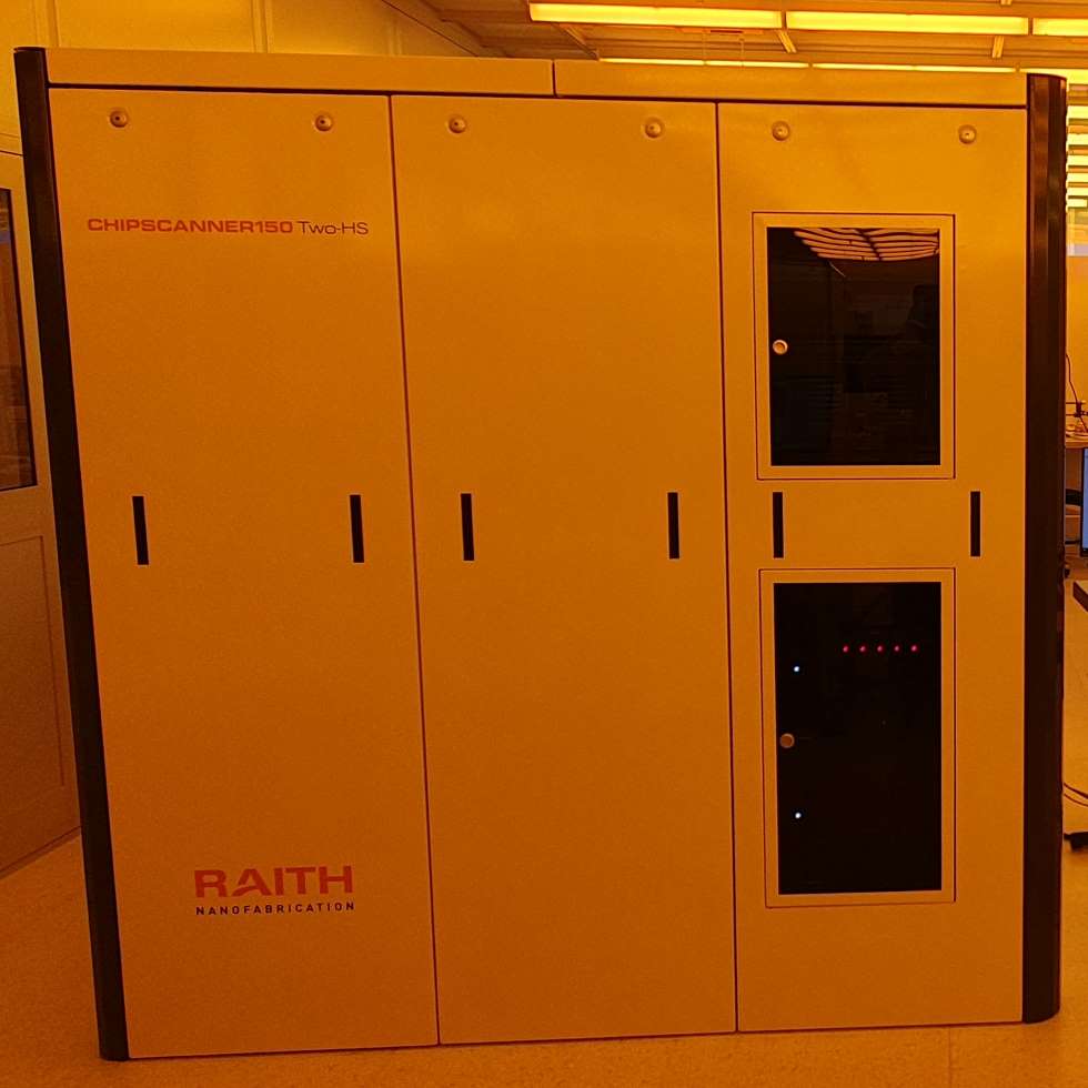
– Automatized SEM:
Raith CHIPSCANNER150Two – HS. Interferometric stage combined with auto focusing capabilities for wafer scale metrology and into the depth process development.
Samples: small chips to 6inch
Stage precision: 1nm
Autofocusing: laser reflection algorithm
Detectors: in-lens, SE, angular BSD
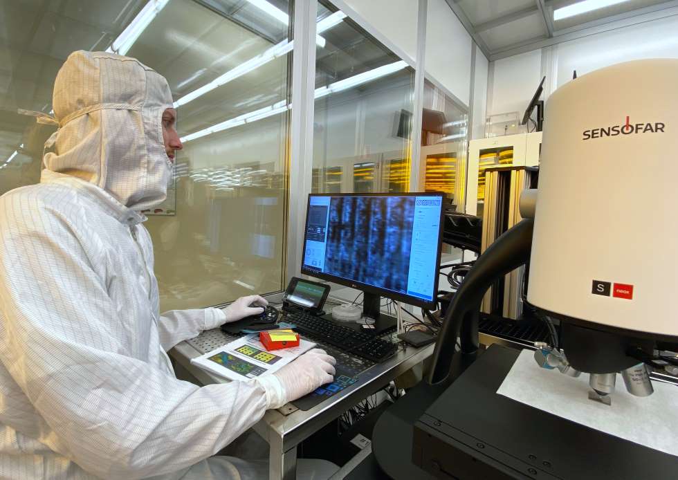
-Optical profilometer (3D features):
Sensofar Sneox. 3D surface metrology is the measurement and characterization of micro- and nano-scale features. This is achieved by capturing the 3D spatial coordinates of points on a surface using a non-destructive optical technique.
Measurement methods: Interferometric/Confocal and AiFocus variation
Samples: Small chips to 150mm wafers. Compatible with irregularly shaped samples and micro-machined parts.
XY resolution: ca.450nm; Z resolution: down to less than 1nm.
Stage precision: Encoded motorized stage with position precision better than 2um.
Objectives: 5X to 100X objectives available (variable numerical apertures)
– Automatic Optical microscope:
Nikon L200ND. Motorized optical microscope with laser autofocus.
Measurements method: Reflected light brightfield/darkfield, reflected light polarization/DIC/Normanski, transmitted light brightfield
Focusing method: A laser autofocus unit using 850 nm light can automatically maintain focus over the sample.
Samples: Small chips to 150mm wafers.
XY resolution: 400nm
Stage precision: Encoded motorized stage with position precision better than 2um.
Objectives: 5X to 100X objectives available (variable NA)
Imaging: high-performance camera for high-resolution low-noise imaging (20Mpixel).
Case study:
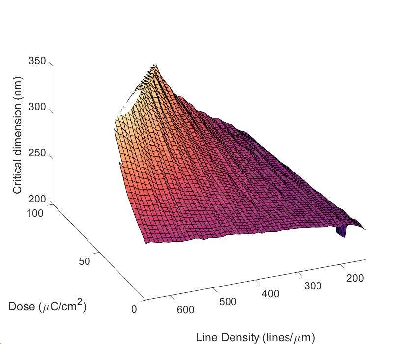
Automatized SEM: size measurements of nanofabricated devices on wafers for improving fabrication yield. Capable to retrieve gdsii files from devices for recursive optimization.
Optical profilometer: measure micromachined parts. Obtain roughness. Measure the 3D etched profile of trenches. Obtain etching uniformity across a wafer.
Optical microscope: find 2D material flake on a preregistered mark. Look for fabrication defects and find their location.
Access Provider / Facilities