Advanced Dry Etching Platform
About
Myfab Chalmers offers several tools and ready-to-use recipes for etching of diverse materials and applications.
Description
The following processes are already established and run within the infrastructure:
– Ion beam milling
– Reactive ion beam milling
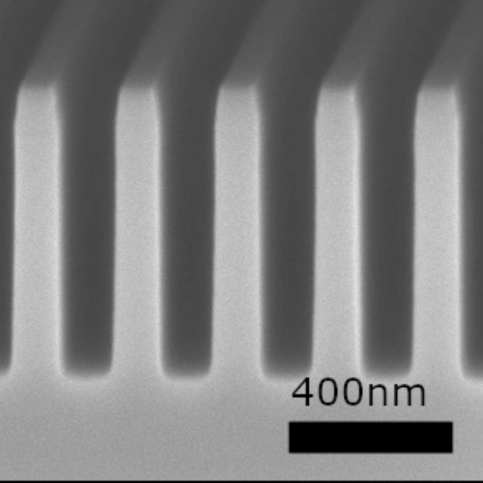
– Deep Si etch (Bosch process) for deep anisotropic etching of Si
– Shallow Si etching with high anisotropy (90deg) and smooth sidewall
– Dielectric etching of SiO2, SiNx
– GaAs etching of high aspect ratio nanostructures
– Compound semiconductor etching at high temperature
– Etching of unconventional materials, such as 2D flakes (TMDC, graphene, …)
– Isotropic Si etching using XeF2 gas vapor
Technical specifications:
Physical etching
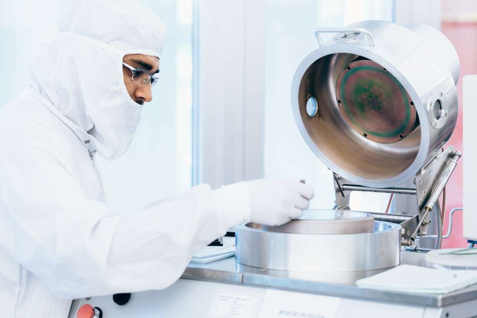
- Oxford Ionfab 300 Plus Ion Beam System. Inert Ar ion milling with SIMS endpoint detection. Etching using LN2 cooling available. 5mm to 100mm wafer.
- Oxford Ionfab 300 Reactive Ion Beam System for Chlorine based reactive ion-beam etching. 5mm to 100mm wafer.
ICP-RIE
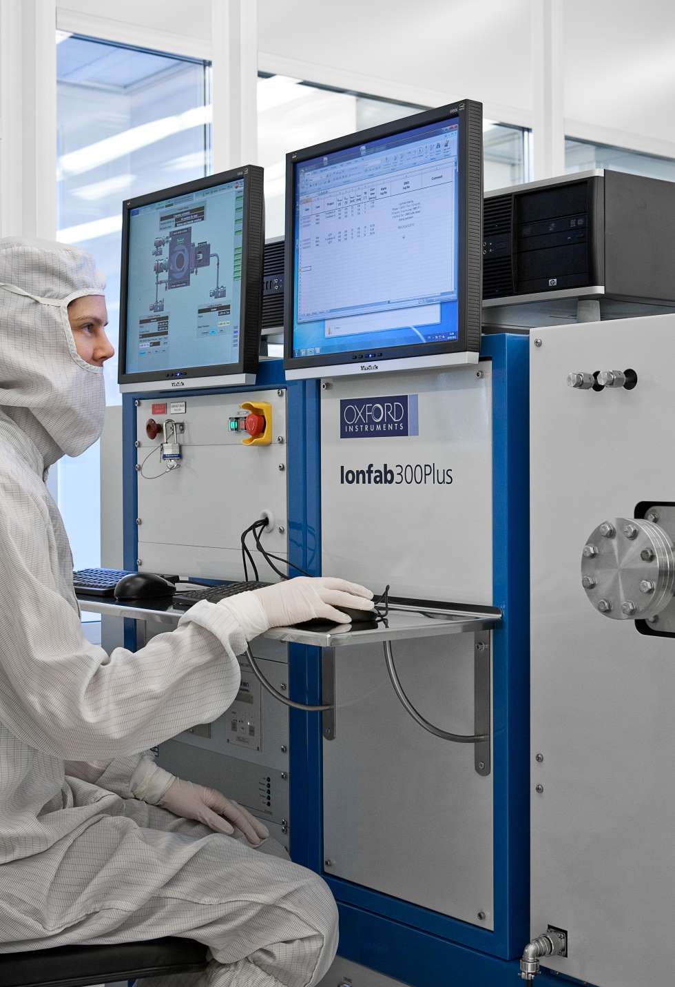
- Oxford PlasmaPro 100 cluster. Double chamber ICP-RIE etching tool with separated Cl-based and F-based etching chemistry. 5mm to 100mm wafers. End-point detection.
- STS ICP-RIE dry etcher with load-lock. HBr, Cl and SF6 etching gases. 5mm to 100mm wafers. High temperature stage for compound semiconductor etching. End-point detection.
- Oxford Estrella for deep Si etch (Bosch Process). 5mm to 150mm wafers. Electrostatic clamp and substrate temperature control.
Vapor etching
- Memstar XeF2 vapor release etching allows dry isotropic etching of Si at μm/min etch rates. 5mm to 150mm wafer.
Access Provider / Facilities
Chalmers University


