Cleanroom Characterization
About
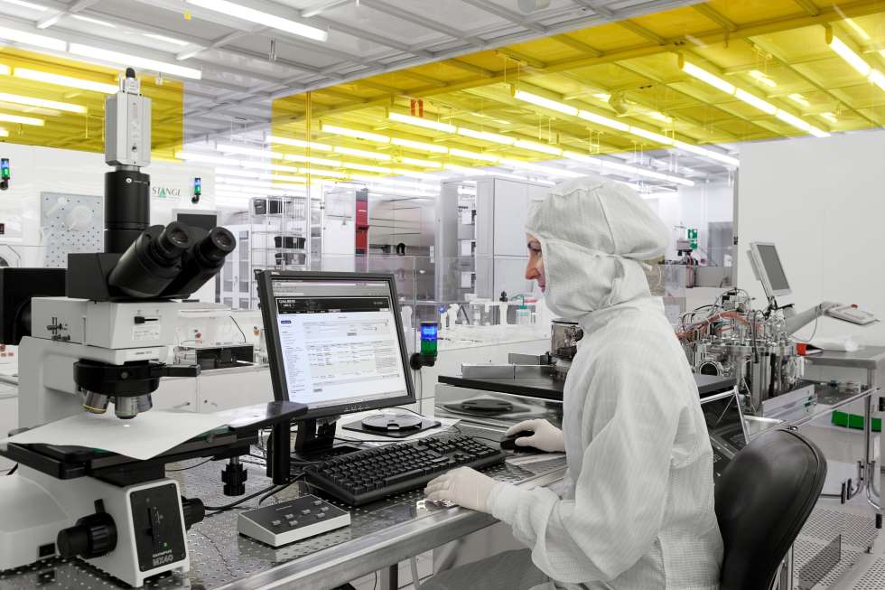
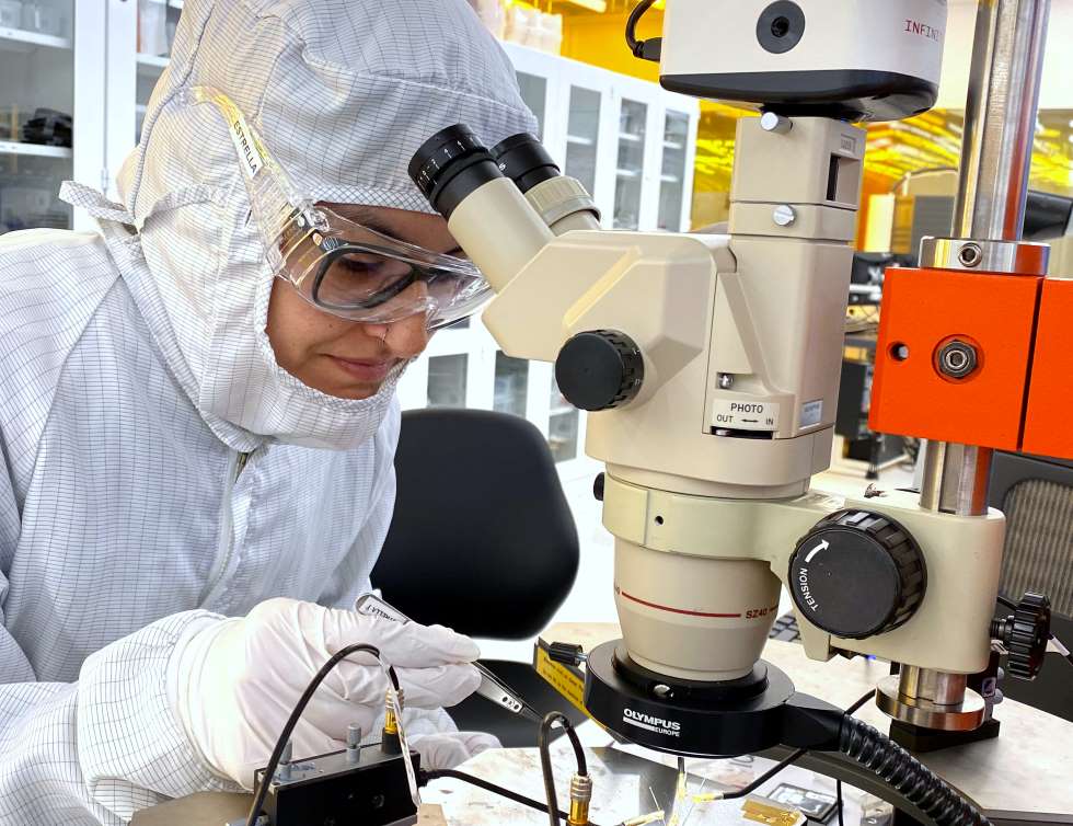
Myfab Chalmers offers a range of characterization tools for fabricated devices. Scanning electron microscope (SEM), Atomic Force microscope (AFM), Spectroscopic Ellipsometer, Raman microscope, Optical microscope, Optical and stylus profilometer, White Light reflectometer.
Description
SEM: Zeiss Supra 60VP, 8inch wafer compatible, EDX detector
Atomic Force microscope: Bruker Dimension ICON. Closed-loop AFM/SPM system.
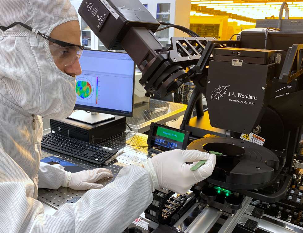
Spectroscopic Ellipsometer: Woolam ellipsometer RC2. Full Muller matrix possible. Automatized mapping and analysis.
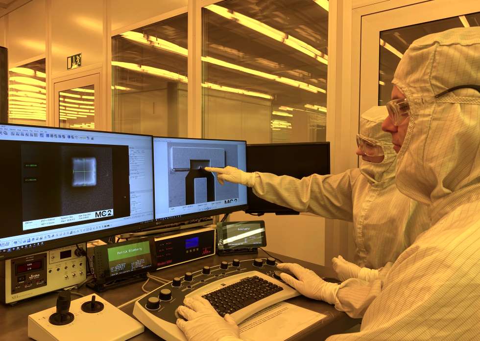
White light reflectometer: ThetaMetrisis
Raman microscope: Horiba Xplora, 638nm laser. 600, 1200 and 1800lines/mm grating
Technical specifications:
- SEM: Zeiss Supra 60VP, 8inch wafer compatible, EDX detector. Resolution down to 1nm
- Atomic Force microscope: Bruker Dimension ICON. Closed-loop AFM/SPM system. Compatible with 8inch wafers, 90um scan range and different scanning modes possible (indentention, STM, MGM, EFM, …).
- Spectroscopic Ellipsometer: Woolam ellipsometer RC2. Wavelength: 245nm to 2500nm. Full Muller matrix possible. Automatized mapping and analysis. 150mm wafer compatible. Temperature controlled stage (RT to 200deg C). Microscopot (150um spot size).
- White light reflectometer: ThetaMetrisis. Wavelength: 220-850nm. Optical film thickness measurement based on reflected white light spectroscopy. Measurement area: 100um. 4inch automatized stage. Fidelity marker recognition possible.
- Raman microscope: Horiba Xplora, 638nm laser. 600, 1200 and 1800lines/mm grating
Access Provider / Facilities
Chalmers University


