Tag Archive for: Deposition of conventional spintronic materials by Sputtering Ion Beam Etching with in situ XPS analysis
 https://infrachip.eu/wp-content/uploads/2024/04/17-CNRS_FMNT_SPIN2D_SPINTEC.jpg
671
980
devinf20
https://infrachip.eu/wp-content/uploads/2024/01/infrachip-logo-3.png
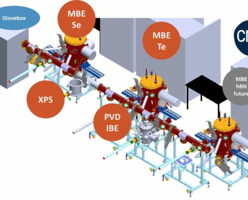
devinf202024-04-12 10:51:402024-05-22 08:17:55Molecular Beam Epitaxy (MBE) for spintronics
https://infrachip.eu/wp-content/uploads/2024/04/17-CNRS_FMNT_SPIN2D_SPINTEC.jpg
671
980
devinf20
https://infrachip.eu/wp-content/uploads/2024/01/infrachip-logo-3.png
devinf202024-04-12 10:51:402024-05-22 08:17:55Molecular Beam Epitaxy (MBE) for spintronics