Molecular Beam Epitaxy (MBE) for spintronics
About
Molecular Beam Epitaxy (MBE) for spintronics - the SPIN2D platform consists in a cluster of Molecular Beam Epitaxy reactors dedicated to the growth of 2D materials, especially transition metal (di)chalcogenides (TMDC) and topological insulators (TI), with in situ characterization tools. The platform counts also with the extended expertise on the growth and characterisation of these materials.
Description
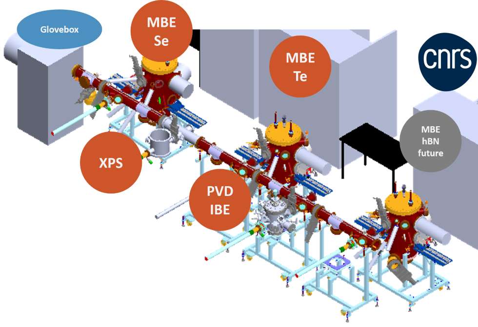
The Molecular Beam Epitaxy (MBE) for spintronics – SPIN2D platform consists of two MBE chambers connected by UHV linear tunnel, together with X-ray Photoemission Spectroscopy (XPS), ion beam etching (IBE) and Sputtering (PVD) systems. These equipment allows the growth MX materials (M=Mo,W,Pt, Fe, Ge, Sn, InSe… and X =Se,Te), ternary materials (for example FeGeTe) and their van der Waals heterostructures.
Many types of TMDC and TI thin film combinations can be grown, from sub-monolayer to several layers thickness with monolayer control, considering the 12 effusion cells and 4 e-gun evaporators. Conventional spintronic materials (as CoFeB, Pt, MgO, Al) can also be combined using an attached PVD chamber. The layer thickness is accurately monitored thanks to quartz microbalances and RHEED (Reflection High Energy Electron Diffraction) oscillations. The surface quality is also monitored during the growth by electron diffraction.
Additionally, in situ XPS allows to probe the chemical environment of each element. The quality of the layers were already systematically checked by advanced characterization tools (HR X-ray diffraction, AFM, Raman spectroscopy and TEM). A long-standing experience allows the growth of TMDC on various substrates, e.g. MoSe2 and WSe2 on graphene and mica.
Technical specifications:
2 MBEs (in-house design), each containing:
6 effusion cells (1 cracker) – feedback control by Temperature
2 e-guns (each 5 pockets) – feedback controlled by Quartz balance
Electron diffraction system (RHEED)
Sample heater (1000°C), Gas analyzer
Some materials available: Fe, Co, Ni, Ge, Te, Se, CaF2, SrF2, Pt, Au, Sn, Sb, V, Hf, Nb, Al, Pd, W, Mo, CoFeB, MgO. 2D layers with monolayer control and high crystallinity: WSe2, MoSe2, PtSe2, VSe2, Bi2Se3 on graphene and mica with the possibility of wet transfer on other substrate. Well-stablished growth of FexGeTe, CrxTe and Bi2Te3 in different substrates.
Sputtering (PVD) – 4 magnetrons (3 DC + 1RF) – Al, AlOx, MgO, Pt, CoFeB…
XPS – Staib Instruments – DESA150 (energy range 0 eV to 2500 eV), Al/Mg X-ray source
Ion Beam Etching – Ar
Case study:
A user would like to develop a new 2D material or van der Waals heterostructure on a specific substrate for scientific or technological purpose. For this, the user brings the substrate and the platform team develops the epitaxial growth of the 2D material/vdW heterostructure on top. Another approach could be the transfer of an epitaxial layer onto a substrate of interest. In the same way, the user brings the substrate, the platform team grows the epitaxial 2D layer or vdW heterostructure and then carries out the transfer (wet) onto the user’s substrate. Beyond 2D materials, the platform can be also used to study surface recover process using IBE, XPS, heat treatment with RHEED evaluation together with the deposition of conventional spintronic materials by sputtering.
Optional:
Dau, M. T. et al. ACS Nano 12, 2319–2331 (2018) doi:10.1021/acsnano.7b07446.
Vergnaud, C. et al. Nanotechnology 31, 255602 (2020) doi:10.1088/1361-6528/ab80fe.
Abdukayumov, K. et al. Adv. Mater. 2304243 (2023) doi:10.1002/adma.202304243.
Guillet, Q. et al. Phys. Rev. Mater. 7, 054005 (2023) doi:10.1103/PhysRevMaterials.7.054005

