Tag Archive for: optical lithography
 https://infrachip.eu/wp-content/uploads/2024/07/21-1.png
226
312
Mathilde Bétend
https://infrachip.eu/wp-content/uploads/2024/01/infrachip-logo-3.png
Mathilde Bétend2024-07-23 15:02:442024-07-24 06:55:29Photolithography
https://infrachip.eu/wp-content/uploads/2024/07/21-1.png
226
312
Mathilde Bétend
https://infrachip.eu/wp-content/uploads/2024/01/infrachip-logo-3.png
Mathilde Bétend2024-07-23 15:02:442024-07-24 06:55:29Photolithography
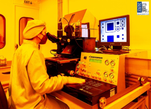
 https://infrachip.eu/wp-content/uploads/2024/04/1_1_main.jpg
676
980
devinf20
https://infrachip.eu/wp-content/uploads/2024/01/infrachip-logo-3.png
devinf202024-04-11 09:06:292024-04-11 13:53:42Cleanroom Broad Fabrication Platform
https://infrachip.eu/wp-content/uploads/2024/04/1_1_main.jpg
676
980
devinf20
https://infrachip.eu/wp-content/uploads/2024/01/infrachip-logo-3.png
devinf202024-04-11 09:06:292024-04-11 13:53:42Cleanroom Broad Fabrication Platform