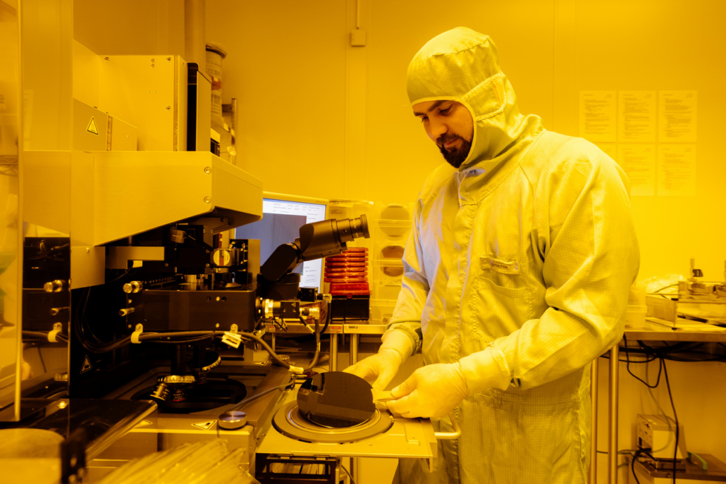
Advanced Lithography Tool
About
Electron Beam Lithography(EBL): Raith EBPG 5200 Photolithography(PL): Semi-Automatic Mask Aligner EVG-420, Canon i-Line Stepper FPA3000 i5+, Automatic Resist Coater and Developer EVG-150 & -SÜSS Microtec RCD8 Nano Imprint Lithography(NIL):, SÜSS MicroTec SCIL UV System MA8
Description
EBL: A Pioneering Maskless Technology for reaching up to sub 10nm resolution. AMO offers a wide range of readily available EBL processes on many different substrate types. Smallest feature size of 50nm on substrate sizes from 10x10mm2 up to 8” Wafer with etch depth up to 1000nm. Fabrication of high aspect ratio nanostructures using super critical resist drying. Single/Dense line resolution of ~10 nm/ ~25 nm.
Photolithography:
Mask Aligner with smallest feature size of 2 µm on Wafers up to 8”.
I-Line Stepper with smallest feature size of 500nm on 6” Wafer only.
Interference Lithography (IL): For precision stitching free gratings with minimum features size of 50nm. Fixed Angle and Variable Angle IL on Silicon and Quartz substrates. Wafer size up to 6” and for selected configurations on 8”.
NIL: Nano Imprint Lithography of 3D structures with minimal feature size of 100nm on substrate sizes from 20x20mm² up to 8” wafers
NIL-Master Fabrication: Advanced Master using Mix-Match between i-line and EBL lithography. Multi-level-masters for 3D applications.
Technical specifications:
EBL: Positive tone Resist (PMMA, UV6) for Sub 15nm or Negative tone Resist (HSQ, UVN30) for sub 10nm using 50kV and 100kV Acceleration voltage. Active patterned area limited by writing time.
PL: Active patterned area up to full substrate, Substrate Material Silicon or Fused silica with thickness 500-650µm.
IL: Exposure Wavelength of 266nm, Minimum feature size of 50nm, Pitch 150/180nm for Fixed Angle IL or 300-2500nm for Variable Angle IL.
Access Provider / Facilities


