Atomic Force Microscope
About
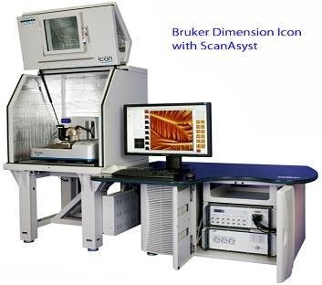
Bruker Atomic Force Microscope (AFM) – Dimension Icon
Description
The Dimension Icon from Bruker performs many scanning probe microscopy operations including Tapping Mode, Contact Mode, Force Spectroscopy, Surface Potential, and Piezoresponse Microscopy.
With Peak Force Tapping, high-resolution images can be acquired in a matter of minutes and for multiple samples if required. Peak force tapping also allows the user to collect nano-mechanical information (e.g. friction, adhesion, deformation) as it scans the materials surface and correlate that with the AFM image. A collection of nano-electrical modes is available with the system, some of which include Kelvin Probe Force Microscopy (KPFM), Scanning Spreading Resistance Microscopy (SSRM), Scanning Capacitance Microscopy (SCM) and Peak Force-TUNA (C-AFM).
These modes can be combined with a feature called DataCube whereby the user can examine the samples characteristics in more detail – e.g. Correlated electrical & mechanical properties in a single measurement.
Technical specifications:
Wafer size: Up to 200mm wafers
Temperature Range: Room Temperature
Fully Automated: Single Wafer Only
RF on Wafer characterisation: No
Case study:
A user is developing nano-scale meta lenses. Thin film (115nm) of amorphous silicon (a-Si) is deposited on pyrex. To create an e-beam mask and etching mask a ZEP resist was applied to the sample by a spinner. The metalenses are fabricated using e-beam lithography. AFM is then used to study the surface of the metalalenses. The metalens has a high numerical aperture and focuses laser light with a wavelength of 532nm into a subwavelength light ring.
Optional:
AFM (3D Virtual Tour)
Access Provider / Facilities