FIB-STEM
About
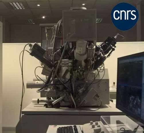
This tool consists of a scanning electronic microscope SEM equipped with a focalized ion beam FIB enabling the milling of materials
Description
Imaging secondary electrons SE and back scattered electrons BSE is possible in-situ thanks to various detectors such as ETD, TLD, CBS ; as well as a STEM detector enabling nanometric resolution.
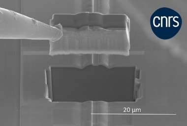
Using a focused gallium ion beam, this equipment enables the preparation of slides by FIB milling,
In addition, the use of focused ion beam enables the ablation of all materials, as well as the deposition of platinum or TEOS, in micron-scale dimensions.
This tool is particularly useful for thinning lamella for ex-situ TEM analysis (EDX, EELS, HRTEM…)
Technical specifications:
The samples we can process are cleaved parts from wafer-based microelectronics manufacture. Samples that can be passed must not exceed 25 mm in diameter and 5 mm high.
Features:
E-beam: 350 V – 30 kV ; 1.6 pA – 100 nA
I-beam: 500 V – 30 kV ; 0.1 pA – 65 nA
Rotation stage 360° – Tilt 58°
Equipped with micromanipulator to relocate the sampling to a TEM grid.
Retractable STEM detector with BF/DF/HAADF segments.
Case study:
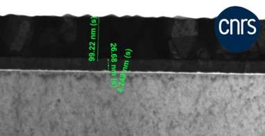
A user may need information on the quality of a manufacturing process step by visualizing a cross-section of its stack, with sub-micron resolution. A better degree of resolution is provided by thinning the sample down to 100 nm thickness, allowing enough electrons to pass through the sample at 30kV to reach the STEM detector; the resolution is then 4 nm.

