Photolithography
About
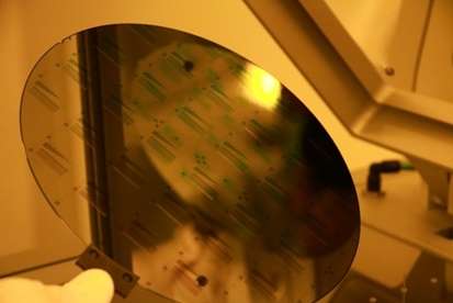
UV photolithography process with um resolution for patterning the predefined shapes in a photoresist.
Description
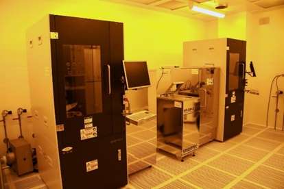
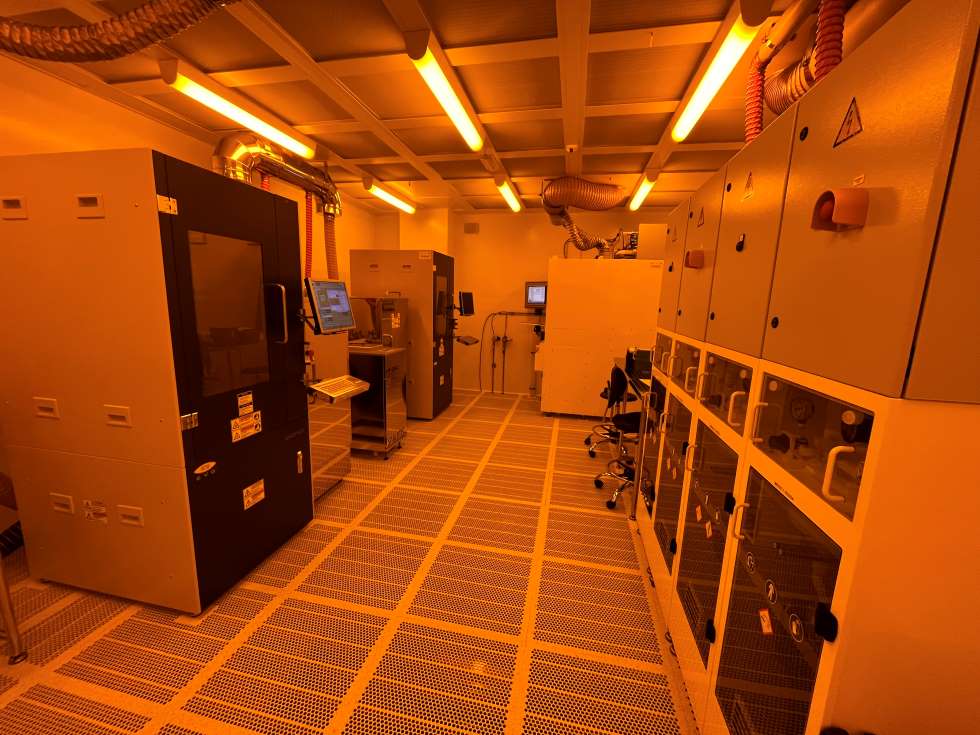
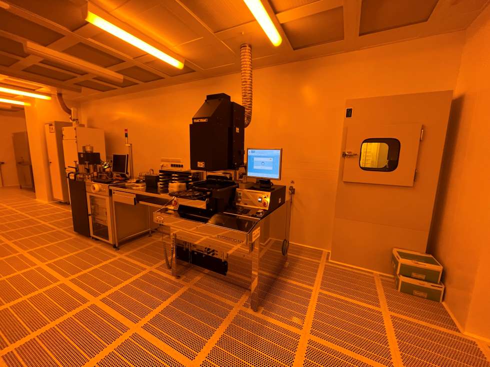
We offer the complete photolithography process, starting from substrate preparation, spin-coating of the resist layer, exposure and development, and hardening. Top-side (TSA) and back-side (BSA) alignment are available (EVG6200NT/200/TB). Repeatable semiautomatic coating and development process (EVG101). Positive and negative tone resists are available for various applications.
Technical specifications:
• working with round substrates up to 200 mm (50 mm/2″, 100 mm/4″, 150 mm/6″, 200 mm/8″) and pieces no smaller than 10 mm x 10 mm,
• top-side alignment (TSA) with an accuracy of 0.5 µm and the back-side alignment (BSA) with an accuracy of 1.0 µm,
• exposing by proximity, contact (soft contact, hard contact), and vacuum contact,
• compatibility with mask sizes of 2.5″x2.5″, 5″x5″, 7″x7″, 9″x9″,
• possible exposure wavelength: 365nm, 434nm,
• exposure in constant-time and constant-dose mode, also constant-dosage mode also in intervals.
Case study:
A user would like to perform a photolithography process to pattern a predefined shape (e.g., waveguide) onto a semiconductor substrate for further processing steps (etching, deposition, etc.).
Access Provider / Facilities