Piezoelectric Al1-xScxN thin-film stack
About
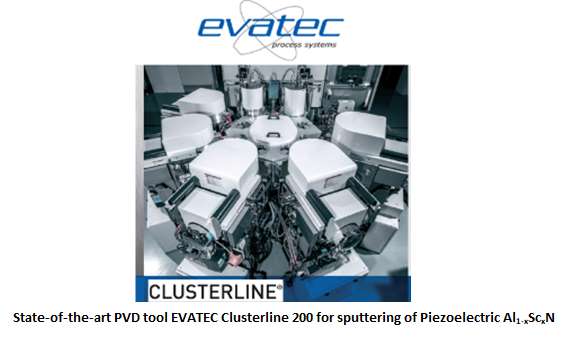
Tyndall National Institute offers Piezoelectric Al1-xScxN thin-film with Sc concentration of 6%, 12% and 27% (i.e. x = 0.06, 0.12 and 0.27), deposited on 100 mm (4 inch) and/or 200 mm (8 inch) Standard Silicon, High-resistivity Silicon, heavily-doped Silicon and Silicon-on-insulator (SOI) substrates. The Al1-xScxN thin-films are deposited using a state-of-the-art multi-chamber magnetron sputtering tool called Evatec Clusterline 200.
Description
In the rapidly evolving field of advanced materials science, the development and deposition of piezoelectric materials, particularly Scadium-doped Aluminium Nitride (Al1-xScxN), have garnered significant attention due to their remarkable properties and wide range of applications. Tyndall National Institute stands at the forefront of this technological advancement by offering high-quality Piezoelectric Al1-xScxN thin-film deposition services. This service is catered to a spectrum of Sc concentrations—specifically, 6%, 12%, and 27% (x = 0.06, 0.12, and 0.27)—to meet diverse research and industrial requirements. The Al1-xScxN thin films are meticulously deposited on various substrates including 100 mm (4 inch) and 200 mm (8 inch) standard silicon, high-resistivity silicon, heavily-doped silicon, and silicon-on-insulator (SOI) substrates, utilizing the advanced capabilities of the Evatec Clusterline 200, a state-of-the-art multi-chamber magnetron sputtering tool.
Importance of Al1-xScxN as an advanced piezoelectric material
Scandium (Sc)-doped Aluminium Nitride (Al1-xScxN) is a superior ICT material due to its exceptional piezoelectric properties compared to wurtzite AlN while retaining all other similar features, e.g., compatibility with CMOS processes, high-temperature stability, and good mechanical properties [1-4]. These features make Al1-xScxN an extremely promising material for deep-tech applications such as RF communication (5G & 6G) [5, 6], ultrasonic sensors [7, 8], energy harvesting [9], and medical imaging [10]. Recent research has also revealed that epitaxial-quality ultra-thin Al1-xScxN exhibits impressive Ferroelectric properties, opening a new potential avenue towards integration of direct memory with logic transistors [11-15].
Tyndall National Institute’s provision of Piezoelectric Al1-xScxN thin-film deposition services represents a significant step forward in the utilization of advanced piezoelectric materials. By offering customized solutions with varying concentrations of Sc and compatibility with different substrates, Tyndall enables researchers and industries to explore and harness the full potential of Al1-xScxN across a multitude of cutting-edge applications. The deployment of the Evatec Clusterline 200 for the deposition process underscores a commitment to precision, quality, and innovation, ensuring that users receive the best possible outcomes for their specific needs.
Technical specifications:
Piezoelectric Al1-xScxN thin-film details:
a) Scandium concentration in atomic percentage – 6%, 12% and 27% (i.e. x = 0.06, 0.12 and 0.27)
b) Al1-xScxN Film thickness – minimum 100 nm to maximum 1.5 µm
c) Al1-xScxN Crystal orientation – C axis (0002)
d) Al1-xScxN thin-film FWHM ≤ 2°
e) Substrate used for deposition – Standard Silicon, High-resistivity silicon, Heavily-doped silicon, and Silicon-on-Insulator (SOI)
f) Substrate diameter – 100 mm (4 inch) and 200 mm (8 inch)
g) Thickness variation across wafer – ± 5%
h) Scandium concentration variation across wafer – ± 10%
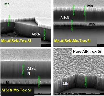
Piezoelectric Al1-xScxN Stack details: Depositing alternate layers of Al1-xScxN thin films and Mo electrode layers can create piezoelectric stacks. The offered details of the stacks are as follows –
a) Full stack with Tox: Mo – Al1-xScxN – Mo – Seed – Tox – Silicon
b) Full stack without Tox: Mo – Al1-xScxN – Mo – Seed – Silicon
c) Bottom Mo stack with Tox: Al1-xScxN – Mo – Seed – Tox – Silicon
d) Bottom Mo stack without Tox: Al1-xScxN – Mo – Seed – Silicon
e) Al1-xScxN on Silicon with Tox: Al1-xScxN – Tox – Silicon
f) Al1-xScxN on Silicon without Tox: Al1-xScxN – Silicon
Seed layer: Ultrathin (~ 50 nm) Al1-xScxN layer is used as the seed layer to improve crystal matching.
Optional:
[1] Akiyama, Morito, Keiichi Umeda, Atsushi Honda, and Toshimi Nagase. “Influence of scandium concentration on power generation figure of merit of scandium aluminum nitride thin films.” Applied physics letters 102, no. 2 (2013).
[2] Österlund, Elmeri, Glenn Ross, Miguel A. Caro, Mervi Paulasto-Kröckel, Andreas Hollmann, Manuela Klaus, Matthias Meixner et al. “Stability and residual stresses of sputtered wurtzite AlScN thin films.” Physical Review Materials 5, no. 3 (2021): 035001.
[3] Zukauskaite, Agne. “Piezoelectric Aluminium Scandium Nitride (AIScN) Thin Film.” (2023).
[4] Mertin, Stefan, Bernd Heinz, Oliver Rattunde, Gabriel Christmann, Marc-Alexandre Dubois, Sylvain Nicolay, and Paul Muralt. “Piezoelectric and structural properties of c-axis textured aluminium scandium nitride thin films up to high scandium content.” Surface and Coatings Technology 343 (2018): 2-6.
[5] Wang, Jialin, Mingyo Park, Stefan Mertin, Tuomas Pensala, Farrokh Ayazi, and Azadeh Ansari. “A film bulk acoustic resonator based on ferroelectric aluminum scandium nitride films.” Journal of Microelectromechanical Systems 29, no. 5 (2020): 741-747.
[6] Zou, Yang, Chao Gao, Jie Zhou, Yan Liu, Qinwen Xu, Yuanhang Qu, WenJuan Liu, Jeffrey Bo Woon Soon, Yao Cai, and Chengliang Sun. “Aluminum scandium nitride thin-film bulk acoustic resonators for 5G wideband applications.” Microsystems & Nanoengineering 8, no. 1 (2022): 124.
[7] Yang, Haolin, Meilin Ji, Xueying Xiu, Haochen Lv, Alex Gu, and Songsong Zhang. “AlScN film based piezoelectric micromechanical ultrasonic transducer for an extended long-range detection.” Micromachines 13, no. 11 (2022): 1942.
[8] Bespalova, Kristina, Elmeri Österlund, Glenn Ross, Mervi Paulasto-Kröckel, Abhilash Thanniyil Sebastian, Cyril Baby Karuthedath, Stefan Mertin, and Tuomas Pensala. “Characterization of AlScN-based multilayer systems for Piezoelectric Micromachined Ultrasound Transducer (pMUT) fabrication.” Journal of Microelectromechanical Systems 30, no. 2 (2021): 290-298.
[9] Liu, Yan, Bohao Hu, Yao Cai, Jie Zhou, Wenjuan Liu, Alexander Tovstopyat, Guoqiang Wu, and Chengliang Sun. “Design and performance of scAlN/AlN trapezoidal cantilever-based MEMS piezoelectric energy harvesters.” IEEE Transactions on Electron Devices 68, no. 6 (2021): 2971-2976.
[10] Wang, Yiwei, Lejia Zhang, Baosheng Wang, Junxiang Cai, Yuandong Alex Gu, Liang Lou, Xiong Wang, and Tao Wu. “Microwave-induced thermoacoustic imaging with a multi-cell AlScN piezoelectric micromachined ultrasonic transducer.” Applied Physics Letters 122, no. 13 (2023).
[11] Fichtner, Simon, Niklas Wolff, Fabian Lofink, Lorenz Kienle, and Bernhard Wagner. “AlScN: A III-V semiconductor based ferroelectric.” Journal of Applied Physics 125, no. 11 (2019).
[12] Liu, Xiwen, Dixiong Wang, Kwan-Ho Kim, Keshava Katti, Jeffrey Zheng, Pariasadat Musavigharavi, Jinshui Miao, Eric A. Stach, Roy H. Olsson III, and Deep Jariwala. “Post-CMOS compatible aluminum scandium nitride/2D channel ferroelectric field-effect-transistor memory.” Nano Letters 21, no. 9 (2021): 3753-3761.
[13] Liu, Xiwen, John Ting, Yunfei He, Merrilyn Mercy Adzo Fiagbenu, Jeffrey Zheng, Dixiong Wang, Jonathan Frost et al. “Reconfigurable compute-in-memory on field-programmable ferroelectric diodes.” Nano letters 22, no. 18 (2022): 7690-7698.
[14] Kim, Kwan-Ho, Seyong Oh, Merrilyn Mercy Adzo Fiagbenu, Jeffrey Zheng, Pariasadat Musavigharavi, Pawan Kumar, Nicholas Trainor et al. “Scalable CMOS back-end-of-line-compatible AlScN/two-dimensional channel ferroelectric field-effect transistors.” Nature Nanotechnology (2023): 1-7.
[15] Liu, Xiwen, Jeffrey Zheng, Dixiong Wang, Pariasadat Musavigharavi, Eric A. Stach, Roy Olsson III, and Deep Jariwala. “A CMOS Compatible Aluminum Scandium Nitride-based Ferroelectric Tunnel Junction Memristor.” arXiv preprint arXiv: 2012. 10019 (2020).
Access Provider / Facilities