Electron beam lithography
About
Electron beam lithography is a precise technique for patterning with a nanometer resolution. The pattern can be transferred to the resist directly from the graphic file.
Description
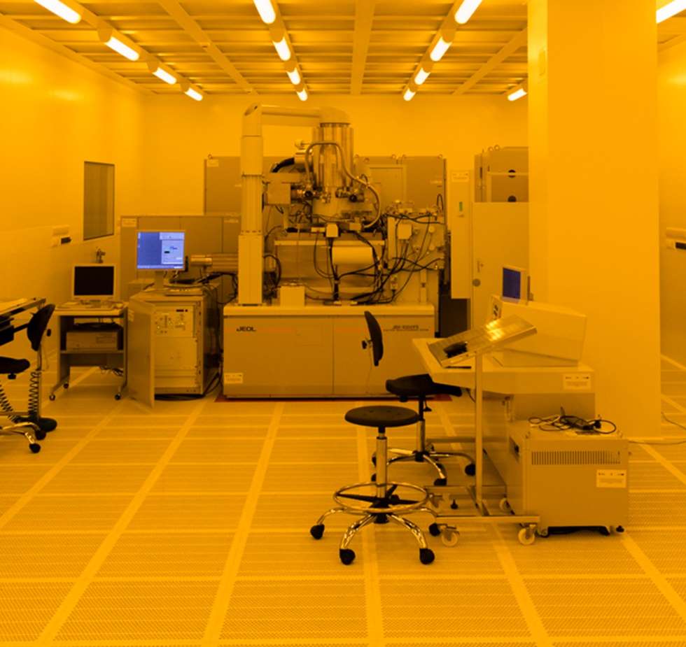
Electron-beam lithography, JBX-9300FX from Jeol, allows patterns to be written directly onto the resist layer, resulting in possible feature dimensions at the level of single nanometers. It gives great flexibility in transferring patterns onto the layer with high precision. This approach eliminates the need to produce and expose the patterns through a mask, as used in photolithography. Thanks to this advantage, quick changes and corrections to the design of the patterns are possible, which is helpful in the research and prototyping phase of structures and devices. The accelerating voltage used in the tool is 100 kV. The minimum diameter of the electron beam used for exposure is less than 5 nm, and the minimum width of the line is less than 20 nm. The maximum exposure area without stitching is 1 mm2.
Technical specifications:
- accelerating voltage: 100 kV,
- exposure beam current range 0.1 – 50 nA.
- exposure field size: 100×100 μm, 500×500 μm and 1000×1000 μm,
- stitching error of the exposure fields ≤ 30 nm,
- possibility to work with various substrates: diameters of 2″, 3″, 4″, 6″, 8″ inches and square 5″ and 7″ substrates; processing of non-standard substrate size by prior agreement,
- standard e-beam resists used in lithography: positive ( 950PMMA A from MicroChem, and ZEP520A from Zeon), negative (XR-1541 from Dow Corning), other resists possible by prior agreement,
- resist layer thickness from several tens of nanometers,
- minimum line width in negative resist from several nm, in positive resist from several tens of nanometers,
- accepted patterns in files: LEDB, GDS OASIS, LTxt, CIF, DXF, PNG,
- preparation and optimization of the exposure process – available software enables, among others, optimal selection and sequence of exposing areas to minimize mapping errors and shorten the processing time, preparation of beam dosage, etc.
Case study:
Due to the high resolution of e-beam lithography, it is possible to fabricate sophisticated structures for photonic and microelectronic devices – grating couplers, arrayed waveguide gratings, distributed Bragg reflectors, or multi-level holograms.
Access Provider / Facilities