Tag Archive for: lithography
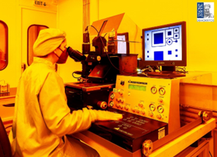
Photolithography
Showroom NCSR Demokritos Devices / Test structures, Dielectric deposition, Dry etching, e-beam lithography, Metal deposition, Optical lithography, Plasma etching, Processing/Fabrication, Wet etching Advanced sensing, Component Neuromorphic computing, Connect, Energy autonomy, Green electronics and substrates, Green sensors, Hybrid SiP/SoC, Photonic sensing, PMU design, Power, Power electronics, Quantum and spin devices engineering, RF components, RF front-end design, Sense, Short-range optical communications, Stretchable and flexible sensors, Sustain, ThinkPhotolithography commonly refers to the pattern transfer of a photomask to a light-sensitive ma...
Access Provider / Facilities

NCSR Demokritos
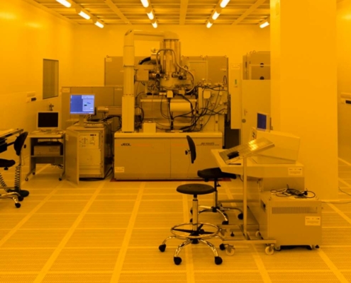
Electron beam lithography
Showroom WUT CEZAMAT e-beam lithography, Processing/Fabrication Energy autonomy, Photonic sensing, Power, SenseElectron beam lithography is a precise technique for patterning with a nanometer resolution. Th...
Access Provider / Facilities

WUT CEZAMAT

Advanced Dry Etching Platform
Showroom Chalmers University Dry etching, Plasma etching, Processing/Fabrication, Wet etching Connect, Power, Power electronics, Quantum and spin devices engineering, RF components, ThinkMyfab Chalmers offers several tools and ready-to-use recipes for etching of diverse materials a...
Access Provider / Facilities

Chalmers University
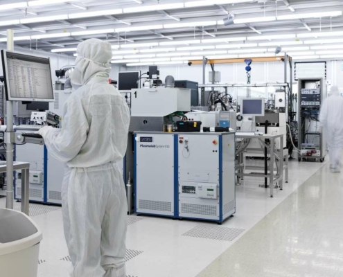
Cleanroom Broad Fabrication Platform
Showroom Chalmers University Dielectric deposition, Dry etching, e-beam lithography, Metal deposition, Metrology / Characterisation, Optical, Optical lithography, Physical/Structural, Plasma etching, Processing/Fabrication, Wet etching Connect, Power, Power electronics, Quantum and spin devices engineering, RF components, ThinkMyfab Chalmers offers a range of cleanrooms processes for full micro/nanofabrication. Depositio...
Access Provider / Facilities

Chalmers University
