Printed thin films and devices

About
UNINOVA offers the access to the entire value chain related to the production and characterization of thin films made through different coating and printing techniques on rigid and flexible substrates. Also, these thin films can be implemented in diverse electronic devices.
Description
Core competences offered:
- Deposition of inks using different deposition techniques for various substrates
- Assisting on ink compatibility for a specific deposition technique
- Thin film material and electrical characterization
- Supporting design to develop patterns for several printing techniques
- Integration of printed thin films in electronic devices, such as transistors and diodes
Major tools:
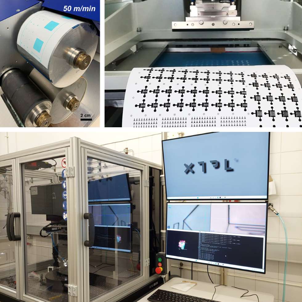
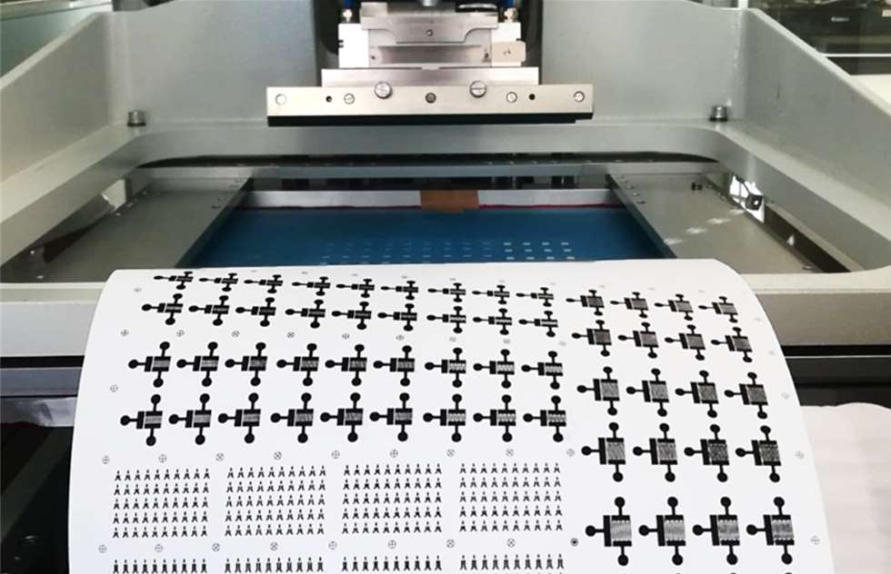
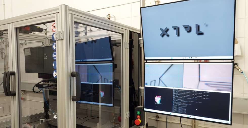
- Deposition techniques: Coating techniques (spin-coating, dip-coating, blade-coating and spray-coating) and Printing techniques (Flexographic printing, Screen printing, Inkjet Printing and XTPL extrusion printing);
- Thin Film Material Characterization: SEM/FIB, XRD, FTIR, XPS, STEM, Raman Spectroscopy, UV-VIS-NIR Spectroscopy, and Optical Microscopy;
- Electrical characterization of circuits, including semiconductor parameter analyzers with IV, pulsed-IV and CV capabilities, oscilloscopes, signal generators, manual probe stations, probe stations with temperature, light and environmental control;
Technical specifications:
Fabrication:
- Deposition on glass or flexible substrates up to A4 size (210 mm x 297 mm) depending on the deposition technique;
- Thin films curing: thermal annealing (up to 450 °C), Infrared oven (up to 300 °C) and UV irradiation (248 nm and 366 nm wavelength), combining thermal annealing and UV irradiation (up to 200 °C)
- Device level (memristors, thin film capacitors and transistors, sensors and biosensors, resistors and heaters) – down to 100×100 µm size. A higher resolution (up 2 µm) can be reached for the XTPL printer to produce conductive electrodes.
Characterization:
- Thin films up to 2.5 cm×2.5 cm size.
- Devices level electrical characterization in probe stations – up to 4” substrate.
Case study:
A user has the requirement to have new inks to test their compatibility with different deposition techniques (coating and printing) to form thin films on various substrates. Some of these thin films concerning their electrical parameters can be implemented in devices (sensors, TFTs, memristors, among others).
Optional:
https://doi.org/10.1002/aelm.201901071
https://doi.org/10.1002/adfm.201606755
https://doi.org/10.1002/admt.202100633
https://doi.org/10.1039/D1TC05465A
https://doi.org/10.1039/D0TC05368F
https://doi.org/10.3390/mi10090601
Access Provider / Facilities

 UNINOVA_offer_thin_film_circuits_for_sensors")

