RESEARCH ACCELERATOR PROGRAMME

Research Accelerator

The Research Accelerator is a short training programme giving early career researchers an on-site introduction to the technology/facilities available through INFRACHIP. For each RA, 6 to 8 participants will be invited.  

INFRACHIP will sponsor PhD students and early-career postdoctoral researchers to attend advanced nanoelectronics technology training courses. This will give them a clear insight into nanofabrication and outline how they can benefit from the INFRACHIP technologies to accelerate their own research. 

An expected outcome of the programme is that sponsored researchers will apply for access at any of the facilities to enhance their studies.

  • Between 2 to 3 days of training at one of the access providers.
  • Discovery of the facilities through visits, lectures on a given topic, discussions with the local experts
  • INFRACHIP will provide financial support towards your travel, accommodation and subsistence expenses
  • PhDs & Early-career researchers (two years maximum passed since you obtained your PhD)
  • You must not be based in the country of the access provider (INL is an exception to this rule)
    Example: a Swedish applicant who is a PhD student in Poland is not allowed to apply to a Research accelerator at CEZAMAT in Poland, but they can apply to one at CHALMERS in Sweden.
  • If you are a PhD student or early career researcher from one of the INFRACHIP access provider, you may not access the RA but have other access means. Please contact us, providing details about your research!
  • Participants who already attended a RA can’t apply again to another RA, but they are welcome to apply to the INFRACHIP programme 🙂

When a Research Accelerator is planned, we will publish it together with the application form on this page. 

If you wish to participate, you will simply have to fill in the application form (identity, motivation, and a CV will be required), then an INFRACHIP panel composed of local staff will make a selection.

Small tip: Don’t tell yourself you have no chance to be selected, if the theme of the RA is important for your research or work and you are motivated, you should apply.

Upcoming Research Accelerators:

Electronic Device Fabrication with 2D Materials


Location Icon

AMO Gmbh, Aachen, Germany

Event Icon

30-31 January 2025

Integrated Power and Energy Systems

Location Icon

Tyndall, Cork, Ireland

Event Icon

5-7 March 2025

Memristors: Materials, Characterization and Applications

Location Icon

NCSR “Demokritos”, Athens, Greece

Event Icon

April 28-30th 2025

Photonic Integrated Circuits: design, technology and characterization

Location Icon

CEZAMAT, Warsaw, Poland

Event Icon

May 26-28th 2025

Automated Metrology

Location Icon

Chalmers, Gothenburg, Sweden

Event Icon

June 24-25th 2025

“Electronic Device Fabrication with 2D Materials” 

30-31 January 2025 – AMO GmbH, Aachen, Germany

Registration closed on November 12th 2024, 10AM CET


This RAP provides a deep dive into the processes, tools, and characterization techniques used in the fabrication of electronic devices with 2D materials like graphene and molybdenum disulfide (MoS₂). Attendees will have the opportunity to apply theoretical knowledge in extensive lab sessions, focusing on practical fabrication and testing of devices.

Key topics

  • Introduction to 2D materials and their unique properties
  • Applications in transistors, sensors, and flexible electronics
  • Hands-on fabrication of 2D material-based electronic devices
  • Characterization techniques (e.g., Raman spectroscopy, AFM, SEM) for assessing material and device properties
  • Lab-focused sessions, giving participants practical experience with state-of-the-art equipment and methods

“Integrated Power and Energy Systems” 

5-7th March 2025 – Tyndall National Institute, Cork, Ireland

Applications closed on December 3rd, 11am CET.


Through this RAP, successful applicants will get an understanding of aspects of Integrated Power and Energy Systems research work that is being carried out by various research groups at Tyndall National Institute. They will understand the technology of MEMS, Energy harvesting and storage and get an overview of integrated magnetics research. Participants will also be introduced to another programme – RISEnergy – from the European Commission, which offers free access to infrastructure for energy systems.

This RAP is organised as part of brokering of services along with RISEnergy and EUROPRACTICE.

Highlights:

  • MEMS Technology
  • Quanscient Multiphysics tool
  • Micromagnetics
  • Thermo Electric Devices
  • Nanomagetics
  • Energy for IoT
  • Tyndall fab and characterization facilities tour
  • OACF lab and other lab tour

“Memristors: Materials, Characterization and Applications” 

April 28-30 2025 – NCSR “Demokritos”, Athens, Greece

Applications closed on January 3rd 10AM CET.

/!\ This RAP is open to PhD students in priority

A large variety of resistive random-access memory (RRAM) technologies are prominent. Nevertheless, a few fulfill the requirements for CMOS integration and meet the commercialization standards. Many dielectrics (e.g., metal oxides, nitrides) have been proposed to realize RRAM. A memristor, a two-terminal nanodevice corresponding to a typical RRAM cell, has garnered substantial attention in recent years due to its distinctive properties and versatile applications. These nanoscale components, characterized by their simplicity of manufacture, scalability in small dimensions, nonvolatile memory capabilities, and adaptability to low-power platforms, offer a wealth of opportunities for technological innovation. Memristors hold great promise in diverse fields, ranging from advanced memory devices and neuromorphic computing to energy-efficient circuits and more.
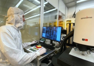
In this short training, participants will discover the cleanroom and characterization labs and dive into memristor through lectures and hands-on expriment.

Key topics:

  • Microelectronics Fabrication Processes
    • Photolithography – Electron Beam Lithography
    • Dry etching – Pattern transfer
    • Low-pressure Chemical Vapor Deposition (LPCVD)
    • Physical Vapor Deposition (PVD)
  • Hands-on training memristor device characterization
    • I-V characterization using semiconductor parameter analyzers
    • Impedance spectroscopy
  • Memristor Applications
    • Resistive RAM
    • Compute-in-memory
    • In sensor computing
    • Neuromorphic computing

“Photonic Integrated Circuits: design, technology and characterization” 

May 26-28th 2025 – CEZAMAT, Warsaw, Poland

Application deadline: 15th February 2025, 10:00 AM CET

This RAP covers a theoretical overview and practical aspects of fabrication and characterization techniques used in Photonic Integrated Circuits (PICs). It will provide lectures and hands-on experience for various aspects of semiconductor technologies utilized in PICs development flow.

We invite you to explore the world of Photonic Integrated Circuits (PICs). CEZAMAT at Warsaw University of Technology invites you to an intensive 3-day workshop designed for students and PhD candidates seeking to expand their expertise in one of today’s most rapidly evolving fields. This workshop offers a unique combination of theoretical insight and hands-on laboratory experience, providing a robust foundation in the design, fabrication and characterization of PICs.

During the training you will:

    • Delve into the fundamentals of PIC design and semiconductor technologies
    • Explore silicon-nitride, SOI, and Ge-on-Si platforms used in advanced research and development
    • Gain practical skills in state-of-the-art fabrication and characterization methods
    • Work directly with advanced equipment in CEZAMAT’s cutting-edge facilities
    • Discover new applications of PICs in bio and environmental sensing systems

“Automated Metrology: Unleashing the power of unprejudiced metrology in University-scale nanofabrication” 

June 24-26th 2025 – Chalmers University of Technology, Gothenburg, Sweden

Application deadline: February 17th, 10AM CET

At Chalmers, we offer hands-on training on advanced automated metrology focusing on specific cases at a wafer scale.

Our cleanroom provides a unique opportunity to access automated tools for image acquisition and data analysis which can be included in your process to improve the tracking of your process status over time and reducing the human factor.

Together, we will explore various real-life practical cases, which will guide your understanding of the capabilities of automated characterization.

Ultimately, we would like to create an awareness of how your processes and samples can profit from automated metrology.

Key topics:

  •  Introduction to automated metrology procedures
  •  Hands-on experience in automated optical microscopy and automated SEM, with focus in particular problems
  • Correlation between image-analysis data and physical properties: the case of Josephson Junctions (JJ) in quantum computing
  • Defect detection and analysis at wafer scale: the case of CVD-grown stressed films
There are currently no events.

Past/Ongoing Research Accelerators:

“Terahertz spectroscopy and imaging”

19-21 November 2024 – CNRS-FMNT: CROMA, Le Bourget-du-Lac, France


This RAP presented the basics of spectroscopy and imaging in the Terahertz (THz) range and give the opportunity to discover the characterization systems available at CROMA Lab. (CNRS-FMNT) on the Terahertz platform (https://infrachip.eu/platera-platform/)

PROGRAMME

Some pictures:

“UV nanoimprinting of microfluidics, microoptics and bionic flexible devices in batch or roll-to-roll”

16-17 September 2024 – JOANNEUM RESEARCH – MATERIALS, Weiz, Austria


UV nanoimprinting is a versatile tool to fabricate components for numerous application. In this Research Accelerator Programme, the participants will get an on-site introduction to various steps involved in the fabrication of surface structures, microoptic or microfluidic devices on small and large scale production.

This RAP relates to the following topics offered in INFRACHIP:

https://infrachip.eu/flexible-microoptics-fab/

https://infrachip.eu/r2r-uv-nanoimprinting/

https://infrachip.eu/flexible-microfluidics-fab/

Programme

“Flexible oxide TFT electronics: from design to circuit fabrication and characterization”

September 4-6th 2024 – UNINOVA, Almada, Portugal

This RAP provided an on-site introduction to the state-of-the-art technology/facilities available at UNINOVA related to flexible oxide thin-film transistors (TFTs). Participants  had contact with the multiple steps required to take oxide TFTs from device level design up to circuit integration, as described here: https://infrachip.eu/thin-film-circuits-for-sensors/

Programme

“Advanced Ink Formulation and Printed Techniques for Emerging Flexible Electronics.” 

May 22nd-24th 2024 – Hellenic Mediterranean University, Greece


  • Module 1: Introduction to Emerging Flexible Electronics
  • Module 2: Ink Formulation for Flexible Electronics and Film Preparation
  • Module 3: Printing & Coating Techniques for Flexible Electronics
  • Module 4: Filament Formation for 3D Printing
  • Module 5: Advanced Techniques for Battery Material Fabrication and Assessment
  • Module 6: Characterization of Solution-Processed Films and Devices