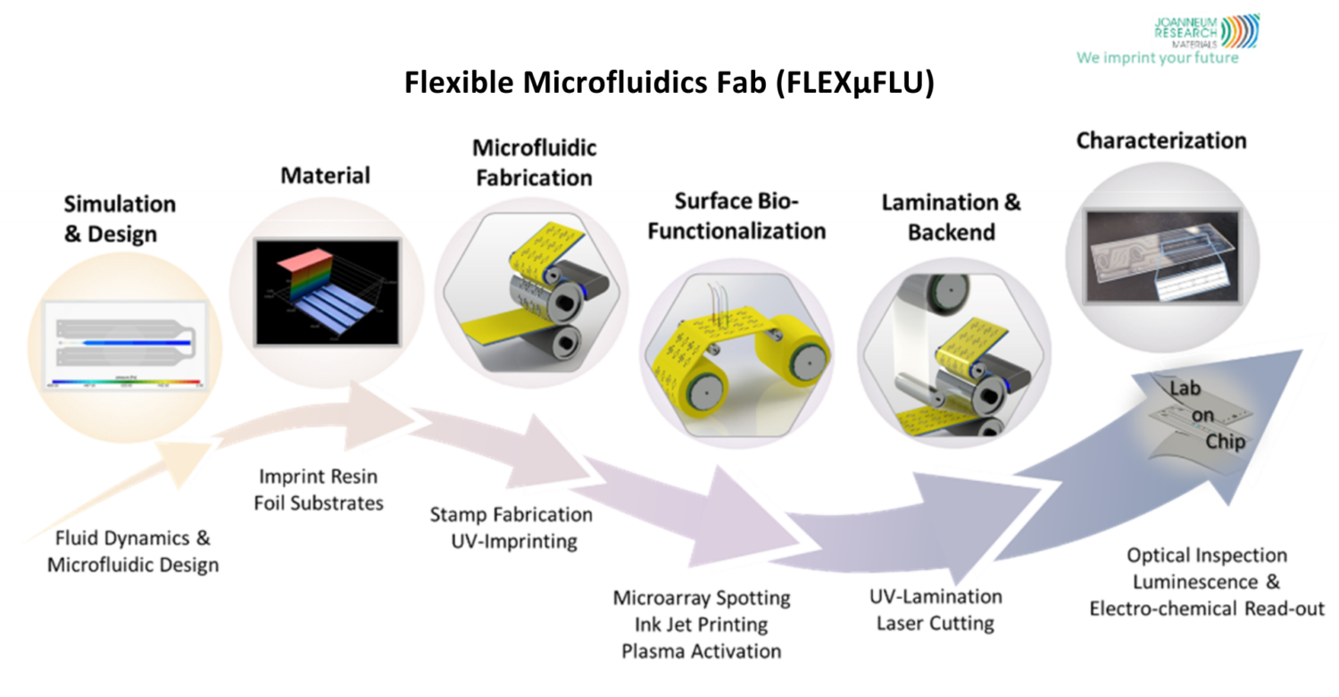
Flexible Microfluidics Fab (FLEXµFLU)
About
Flexible Microfluidics Fab covers the whole development chain for high throughput fabrication of microfluidic “lab-on-foil” chips - Simulation & design: fluid dynamics & microfluidic design - Material selection & development: imprint resin & foil substrate - Microfluidic fabrication: stamp fabrication – UV-imprinting - Surface bio-functionalization: micro array spotting, ink jet printing, plasma activation - Lamination & backend: UV-lamination & laser cutting - Characterization: optical inspection, lluminescence and electro-chemical read-out, surface characterization
Description
The Flexible Microfluidics Fab is made up of six modules to develop and evaluate microfluidic based lab-on-foil chips. These can be used for assay and drug development, point of care consumables, blood sampling or nanoparticle fabrication tools. Our modules cover the whole value chain, starting from simulation and design to characterization and validation of the chips.
We plan the fabrication process together with the user to achieve the desired functionalities and:
– discuss the target specifications and functionalities of the microfluidic based lab on chip system and perform fluid dynamic simulations (Module Simulation & Design)
– make the layout of the microfluidic channel or design the entire “lab-on-foil” chip (Module Simulation & Design)
– select an adequate polymer substrate (refractive index, autofluorescence, recycled material) (Module Material), adapt or develop imprint resins by considering user requirements (surface energy, biocompatibility, cell cytotoxicity, autofluorescence, refractive index, adhesion to substrate). We already have a wide range of imprint resins in our NILcure® family (Module Material)
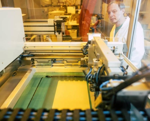
– fabricate the microfluidic channels, starting from mastering processes (photolithography, laser lithography), working stamp fabrication (galvanisation) and (roll-to-roll) UV imprinting (Module Microfluidic Fabrication)
– perform the necessary surface treatment (plasma or Corona activation) and bio-functionalization (deposition of probe molecules via (roll-to-roll) microarray spotting, inkjet printing or aersosoljet printing (Module Surface bio-functionalization)
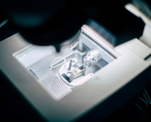
– characterize the properties of imprinted layers by SEM, AFM, surface profiler, tensile tester, contact angle measurements (Module Characterization)
– assemble the (functionalized) microfluidic layer with a cover foil via (roll-to-roll) UV lamination, or application of a screen-printed glue (Module Lamination & Backend)
– use laser cutting for chip singulation and inlet and venting hole definition (Module Lamination & Backend)
– test the functionality of the assembled microfluidic chip with optical inspection, filling tests, luminescence or electrochemical readout tests (Module Characterization)
The modules are offered individually or in a process flow. Please note, that access to the entire process flow might be exhausting and requires therefore splitting into several projects. For further details contact the access provider.
Technical specifications:
Module Microfluidic Simulation & Design
AutoCad, SolidWorks, Comsol, …
Module Microfluidic Fabrication
– Mastering of microfluidic design (channels, wells, valves, …) with photolithography: dry resin available with thickness up to 125 µm, aspect ratio 2:1
– Fabrication of working stamp in in galvanization chamber: up to 6”
– Batch imprinting of microfluidic structures into NILcure®_microfluidic resin formulations optimized for microfluidics on PET, PS or COC polymer substrate
See NILcure® UV-imprint resins
– Continuous imprinting of microfluidic structures into NILcure®_microfluidic resin on polymer substrate rolls by R2R UV Nanoimprinting: max. roll width – 29 cm; roll material: PET; PS or COC; max. channel depth – 200 µm
Module Surface Biofunctionalization
Deposition of nucleic acid or protein probes into (imprinted) microfluidic chip structures by R2R-microarray spotting (Scienion) including plasma activation for immobilization on foil substrates: 4 nozzles in parallel with pL or nL volumes; stop&go operation, R2R foil substrate feeding
Module Lamination
Closing of chips by
- a) R2R UV-lamination with a UV-resin coated cover foil in the R2R UV nanoimprinting machine: R2R scale
see R2R UV-Nanoimprinting
- b) screen printing of adhesives on cover foils followed by lamination under slight pressure: batch scale
see Screen Printer Thieme
Module Backend
Cutting of holes for sample inlet, outlet and venting and singulation of chips by laser processes
-Trotec Laser cutter (CO2 or fibre source)
-Femtosecond Laser
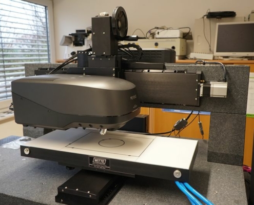
Module Characterization:
Fluorescence Microscopy
Laser scanning microscope: see
Cross section analysis: see
SEM pictures: see
Fluigent for flow tests
Contact angle measurements
Related technology:
Microfluidic Fabrication: NILcure® UV-imprint resins
Microfluidic Fabrication/Lamination: R2R UV-Nanoimprinting
Surface Biofunctionalization: Micro Array Spotter
Lamination: Screen Printer Thieme
Characterization: 3D confocal laser microscope
Characterization: Cryo-Ultramicrotome
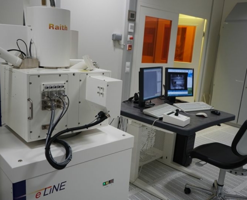
Characterization: RAITH e-line (SEM)
Case study:
An SME in medical or health care industry wants to implement their assay into a flexible microfluidic lab on chip with high throughput fabrication potential. This implementation includes:
(1) a new design taking into account design rules for fabrication and specifications of the assay (2 days). The design can be supported by COMSOL simulations to verify bubble free filling or estimate capillary filling times of the microfluidic channels (5days) .
(2) photolithographic mastering of the microfluidic chip into a dry resin (1day). A photomask, either foil or glass mask, depending on the resolution will be ordered externally. Master up to 6” can be transferred into a working stamp by Joanneum Research (either PDMS (1day) or Ni (2 days))
(3) batch UV imprinting of the microfluidic chip structure with small scale Ni stamp (up to 6”) (2 days). UV resin will be adapted to customers need (5 days).
(4) surface functionalisation of the microfluidic channels with the provided antibodies or sensor probes (by customer) in the spotting machine in batch format (5 days)
(5) batch lamination and hole cutting and chip singulation (3 days)
(6) if design and resin is approved by customer a large area polymer imprinting tool will be fabricated by placing several imprints of a Ni copy of the first Ni stamp on a substrate.
(7) anti-sticking surface functionalization of the polymer stamp (2 days).
(8) production of rolls with such microfluidic chips by R2R-UV nanoimprinting (5 days).
(9) surface functionalisation of the microfluidic channels with the provided antibodies or sensor probes (by customer) in the R2R spotting machine (7 days)
(10) R2R UV lamination of cover foil onto functionalized chip (2 days)
(11) chip singulation and hole cutting (inlet and venting holes) with laser cutter (2 days)
Optional:
- Tören et al., MRS Advances 2021, https://doi.org/10.1557/s43580-021-00064-7
- Tören et al., Lab Chip 20, 4106-4117 (2020)
- Chester et al., ACS Appl. Bio Materials (2020) https://dx.doi.org/10.1021/acsabm.9b00770
P. Remaud, et al., Mater. Chem. Front. 4, 197 (2020)
A. A. K. Das et al., J. Mater. Chem. B 7, 3497 (2019) - Leitgeb et al., ACS Nano 10 (5), 4926 (2016)
Access Provider / Facilities