Flexible Microoptics Fab (FLEXµOPT)
About
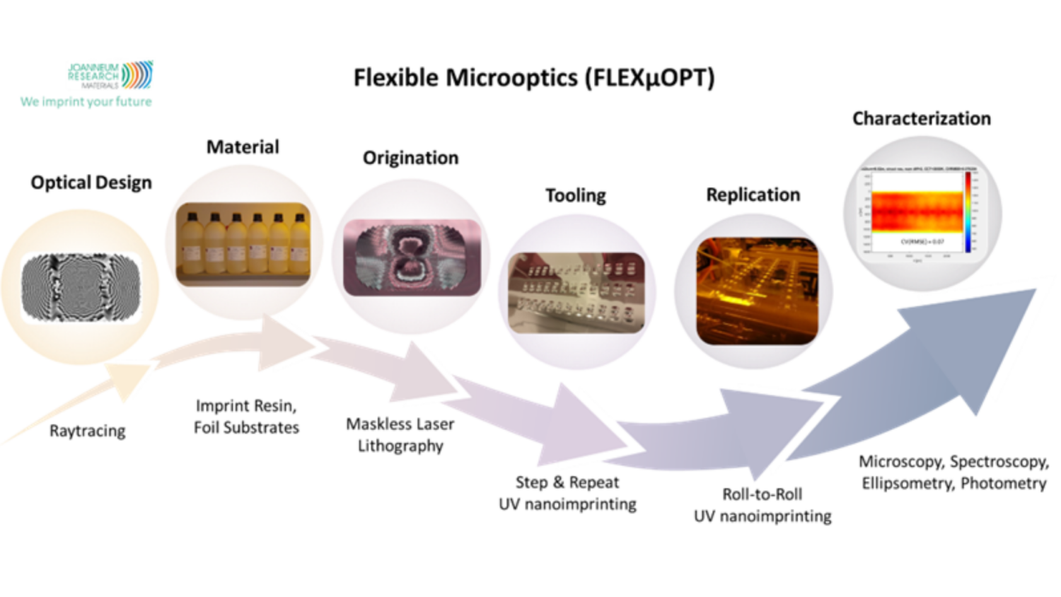
FLEXµOPT covers the whole development chain for 2D-2.5D freeform microoptical elements on flexible substrates - Optical Design: raytracing - Material: imprint resins & foil substrates - Origination: master fabrication by maskless greyscale laser lithography - Tooling: stamp fabrication by step & repeat UV nanoimprinting - Replication: roll-to-roll UV nanoimprinting - Characterization: microscopy, optical spectroscopy, ellipsometry, photometry
Description
FLEXµOPT is made up of six modules to develop and evaluate freeform microoptical elements integrated on flexible substrates that can be used for light management & light guiding in ultrathin luminaires, multi-lens arrays, VR/AR display, photovoltaic modules, or decorative surfaces.
In the Infrachip program, we plan the fabrication process together with the user to achieve the desired functionalities and:
– discuss the target specifications and functionalities of the desired microoptical film (Module Optical Design)
– perform raytracing simulations and design the elements based on the specs (Module Optical Design)
– select an adequate polymer substrate (refractive index, thickness, transparency/absorption, roughness) (Module Material)
– adapt or develop imprint resins by considering the user requirements (surface energy, refractive index, adhesion to substrate, weathering stability, transparency/absorption). We already have a wide range of imprinting resins in our NILcure family available (Module Material).
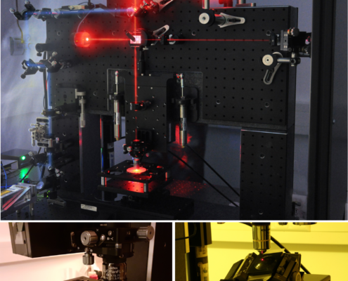
– fabricate the master stamp with the original microoptical structures by maskless greyscale laser lithography in a photoresist on a Si wafer. The structures are based on an optical design provided by the user or are simulated by Joanneum Research (Module Origination)
– fabricate a Ni copy of the master stamp by electroforming (Module Origination)
– fabricate a large-area polymer stamp on a flexible substrate by step & repeat UV nanoimprinting with a working stamp moulded from the Ni copy. The flexible polymer stamp is used as the stamp tool for replication in a roll-to-roll UV nanoimprinting machine (Module Tooling)
– replicate the microoptical structures continuously on a flexible substrate roll at high throughput with roll-to-roll UV nanoimprinting (Module Replication)
– characterize microoptical structures by various microscopes, optical spectroscopy and ellipsometry (Module Characterization)
– test the functionality of microoptical films by photometry (Module Characterization)
The modules are offered individually or in a process flow. Please note, that access to the entire process flow has to be split in several projects that run one after the other. For further details contact the access provider.
Technical specifications:
Module Optical Design
Raytracing by Breault or ASAP
See Raytracing ASAP Breault Research
Module Material
Stamp and product NILcure resin formulations based on acrylates with tuneable properties such as Young’s modulus: 5 MPa- 5 GPa, Surface energy: 15 -70 mN/m, Refractive index: 1.4 – 1.8
Substrates: PET, PC, PMMA, …
See NILcure® UV-imprint resins
Module Origination
Structure definition in a positive-tone photoresist on up to 6” wafers by our self-built maskless greyscale laser lithography setup supporting one and two photon laser lithography
Structure types: 2D – 2.5D
Structure dimensions: minimum lateral structure size – 200 nm, maximum structure depth – 60 µm, aspect ratio – 1:4
Ni galvanization for up to 6” samples
See Maskless Laser Lithography
Module Tooling
Tiling of fields of the mastered microoptical structures by repetitive UV nanoimprinting (step & repeat UV nanoimprinting) with a working stamp in a standard stamp resin on a PET foil.
Substrate area – up to 700 x 380 mm2, positioning accuracy – 3µm
Module Replication
Continuous fabrication of microoptical structures in a product resin (from customer or developed by Joanneum Research) on a polymer film by R2R UV nanoimprinting
Speed – up to 30 m/min, Web width – up to 280 mm, Web material – PET, Cellulose, …
Feature size: down to 50 nm
Characterization:
Microscopy:
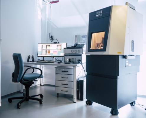
Confocal laser scanning microscope (Keyance): see 3D confocal laser microscope
Scanning electron microscope and Ultramicrotome (JEOL, RAITH Eline): see RAITH e-line (SEM)
Atomic force microscope (Oxford Instruments): see Jupiter AFM
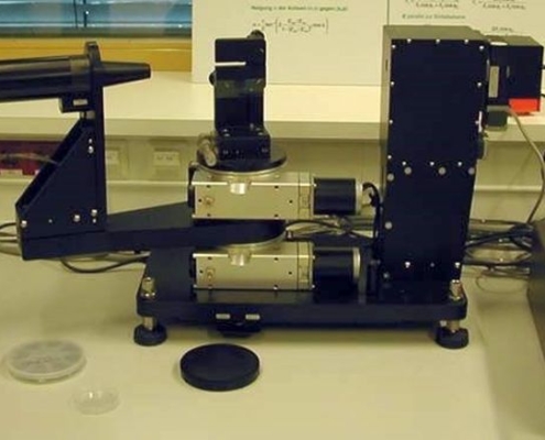
Ellipsometry:
Variable angle and wavelength spectroscopic ellipsometry (Woollam): see Ellipsometer VASE
Spectroscopy:
Fourier – Infrared spectrometer
UV-vis absorption spectrometer
Fluorescence spectrometer
Photometry:
Goniospectrophotometer
Ulbricht Sphere
Related technology:
Optical Design: Raytracing ASAP Breault Research
Material:NILcure® UV-imprint resins
Origination: Maskless Laser Lithography
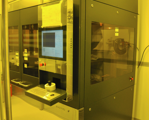
Tooling: Foil Stepper EVG770
Replication: R2R UV-Nanoimprinting
Characterization: 3D confocal laser microscope
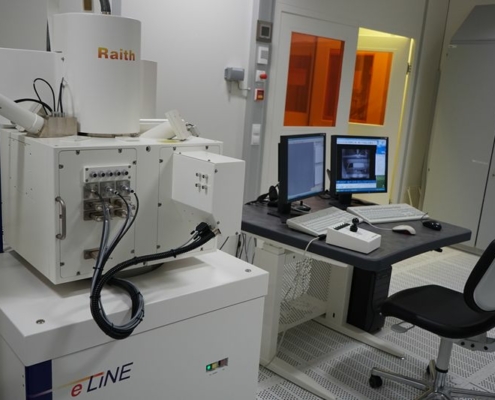
Characterization: RAITH e-line (SEM)
Characterization: Jupiter AFM
Characterization: Ellipsometer VASE
Case study:
An SME operating in the lighting industry wants to improve the performance of its 60 cm long rectangular direct-lit luminaire by reducing the number of LEDs, thus saving costs and energy without compromising the uniformity of the irradiance at the diffuser. The luminaire should remain as thin as possible.
- to take this into account, a polymer film with an array of free-form microlenses only 50 µm high is designed by ray tracing (20 days). 2. such a microlens is then produced by maskless laser lithography (20-40 days, depending on structure complexity). 3. a Ni copy of the template must be produced by electroforming (2 days), from which a working stamp is then formed for the S&R process (2 days). 4. S&R UV nanoimprinting of the microlenses in the desired arrangement (here: stripes) over the target length of 60 cm resulting in a large area polymer stamp with several stripes of these lens elements (20-40 days) 5. anti-sticking surface treatment of the polymer stamp (2 days). 6. production of rolls with stripes of free-form microlenses by R2R UV nanoimprinting (5 days).
Optional:
a.) Publications:
- Keller, LED professional Review 101, 42 (2024)
- Götz et al., ACS Appl. Nano Mater 5, 3434–3449 (2022)
- R. Howell, et al., Optics & Laser Technology 114, 107101 (2021)
- Leiner et al., OSA Continuum 1, 1144 (2018)
- Sommer et al., LED professional Review 67, 50 (2018)
- Kuna et al., J. Photon. Energy 7 (2017)
- Leitgeb et al., ACS Nano 10 (5), 4926 (2016)
- Leiner et al., Proc. of SPIE Vol. 9955, 99550E-3 (2016)
- Leiner et al., Proc. of SPIE Vol. 9889, 988911-7 (2016)
b.) Reference Projects (international):
H2020 projects: Phabulous, ActPhast 4.0, ActPhast 4R, MedPhab
Horizon Europe: Photon Hub, MultiMold, Optimal
Access Provider / Facilities