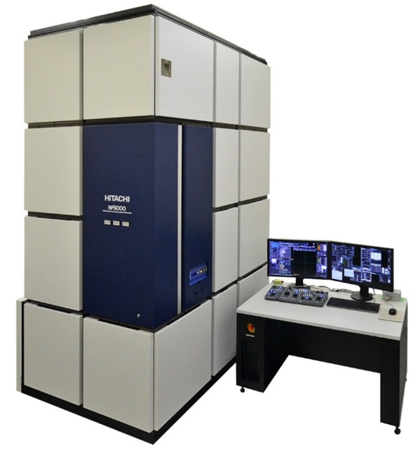
STEM Hitachi HF-5000
About
The HF-5000 transmission electron microscope from Hitachi is a 200 kV aberration-corrected CFE TEM or STEM that provides a robust combination of atomic-resolution imaging and analysis, along with extensive automation and sophisticated in-situ capabilities.
Description
Features:
1 – Hitachi fully automated probe-forming spherical aberration corrector
2 – High-brightness and high-stability cold FE electron gun (Cold FEG)
The high-stability Cold FEG uses a thoroughly redesigned version of Hitachi’s long-established cold field-emission electron source technology. Total system stability has also been optimized in order to achieve sub-Å imaging. The column, power supplies and specimen stage have all been newly designed to offer the very best mechanical and electrical stability. Combining these capabilities with Hitachi’s unique fully-automated probe-forming Cs-corrector, just requiring a single click of a mouse, ensures all users can reach the very best performance quickly and easily.
3 – Ultra-stable column and power supplies for enhanced instrument performance
4 – Simultaneous Cs-corrected SEM & STEM imaging capability with atomic resolution, with ET-type SE detector. This enables the correlation of surface and internal information with insights into the 3D structure of the specimen, without the need to perform 3D tomography.
Additionally, the Cs-corrected SEM image offers higher spatial resolution with more faithful surface information
5 – New high-stability side-entry specimen stage and specimen holders
6 – High-sensitivity and high-throughput EDX detector. On crystalline samples, EDX acquisition can be performed simply with the zone axis aligned, in a single detector configuration.
The large solid angle also means that EDX mapping can be achieved even on beam-sensitive and/or low X-ray yield specimens, including atomic column mapping. High pixel resolution EDX with wide field of view is also achievable, providing large high-resolution datasets.
Technical specifications:
Imaging resolution:
. STEM: 0.078 nm (ADF-STEM image)
. TEM: 0.12 nm (lattice image)
Magnification:
STEM: x8,000,000
TEM: x1,500,00
Specimen stage:
. Specimen size: 3 mm (diameter)
. Specimen transverse: X, Y = ± 1.0 mm, Z = ± 0.4 mm
. Specimen tilt: a = ± 25°, b = ± 35° (Hitachi double-tilt specimen holder)
Case study:
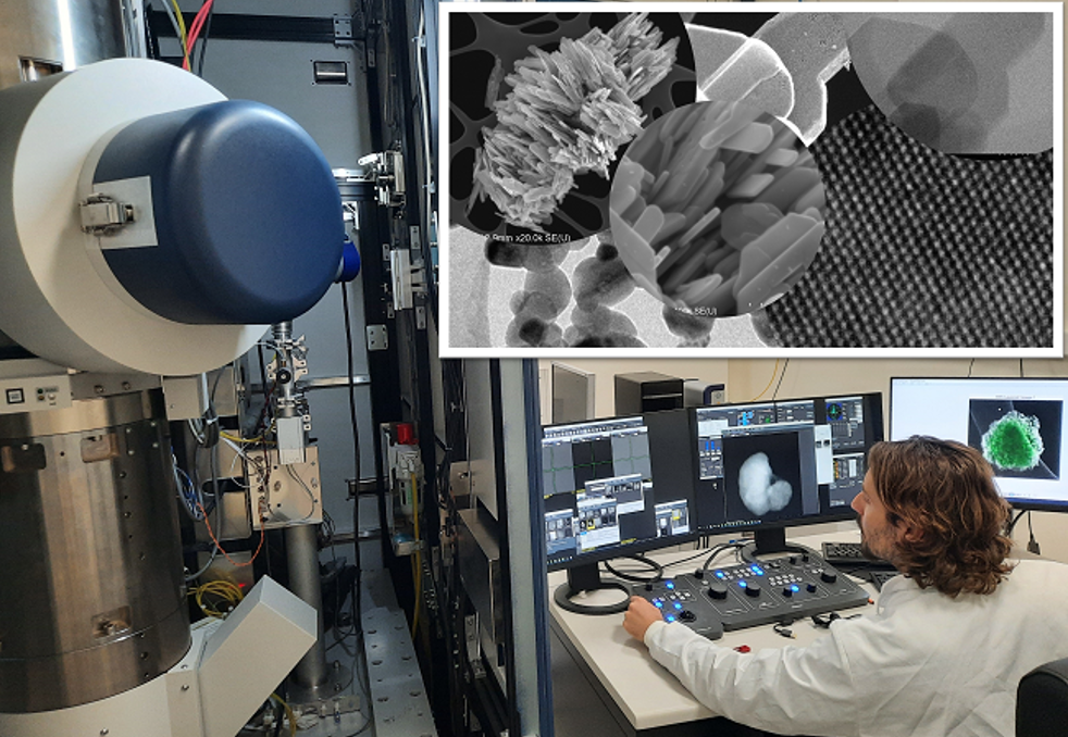
The user has the requirement to have sonicated dispersions to be deposited onto 200-mesh lacey-carbon cooper grids, which is allowed to dry before observation.
Samples are investigated using a STEM from Hitachi HF5000, operating at 200 kV or 60 kV. This is a cold FEG TEM/STEM with a spherical aberration corrector for the probe, and it is equipped with one 100 mm2 EDS detector from Oxford Instruments.
SE-STEM, BF-STEM and Atomic-resolution HAADF-STEM images can be acquired with determination of the FFT.
Optional:
Access Provider / Facilities