Scanning Electron Microscopy
About
UNINOVA offers access to the entire value chain related to SEM analyses of different kinds of samples (thin films, substrates, nanostructures, etc.). Additionally, it is also possible to analyze samples using FIB, EDS, GIS, and in-situ electrical characterization.
Description
Core competences offered:
- Scanning electron microscopic (SEM) imaging of different kind of samples;
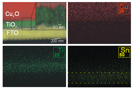
- Energy dispersive X-ray spectroscopy (EDS) for elemental analysis;
- Focused Ion Beam (FIB), which allows, for example, cross-section cuts;
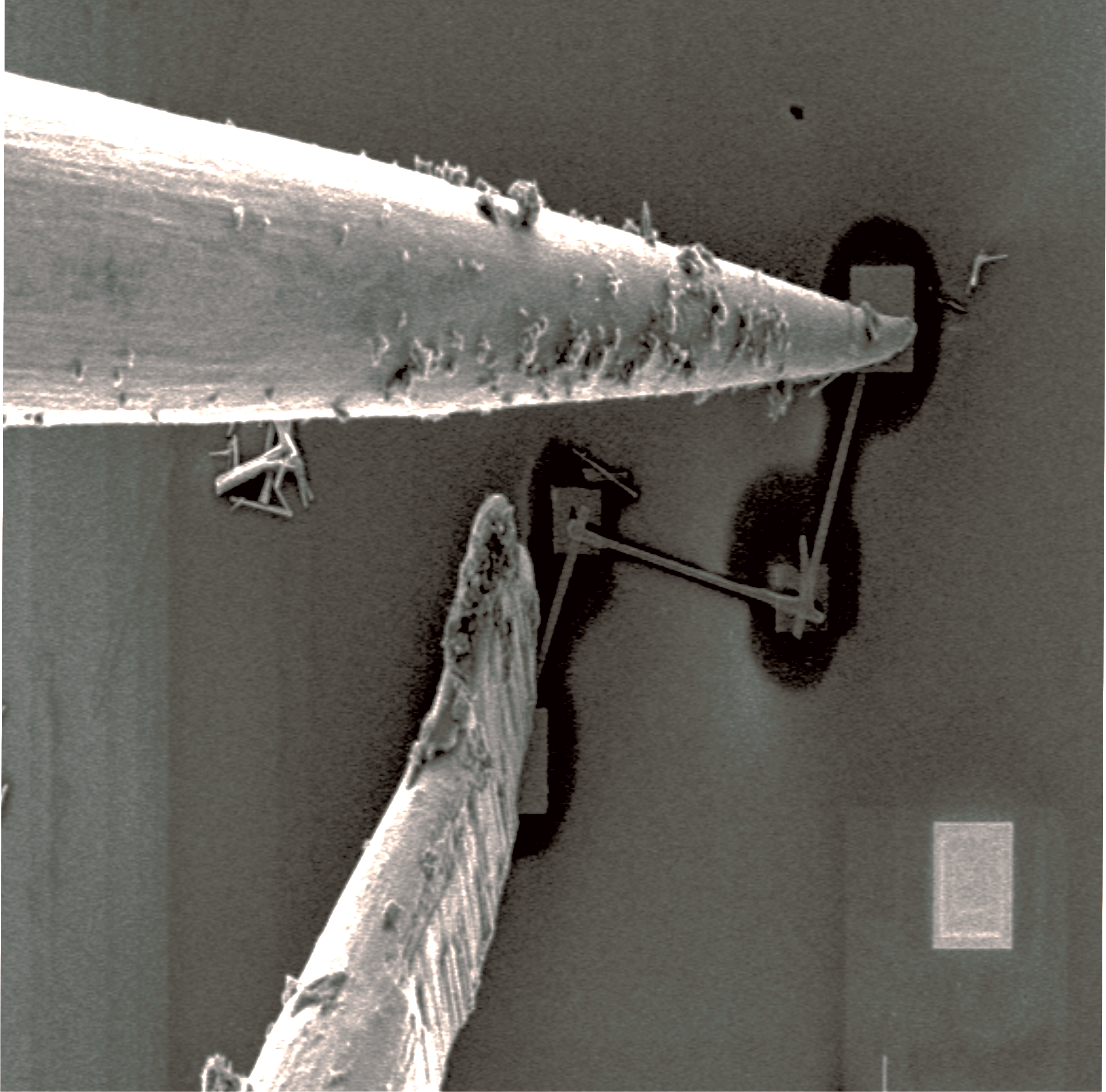
- 4 Kleindiek nanotechnik nanomanipulators for electrical measurements and sample manipulation (e.g., TEM lamella preparation). 4 Triaxial connectors for external semiconductor parameter analyzer (SPA)
- GIS for C, Pt and SiO2 deposition and XeF2 for Si selective etching
Major tools:
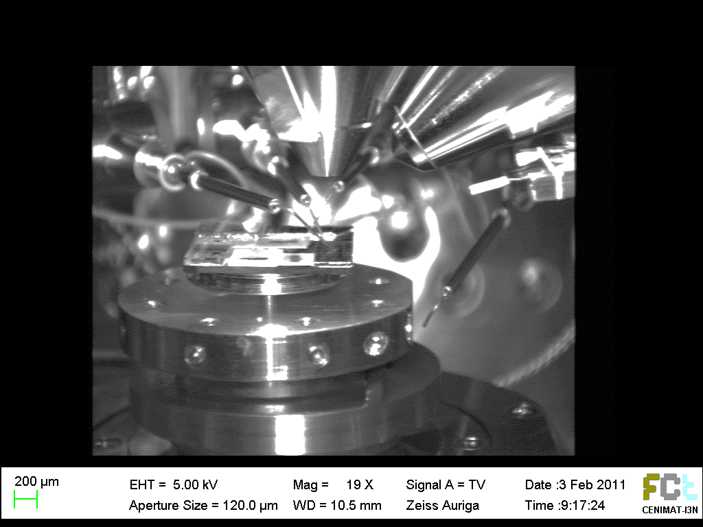
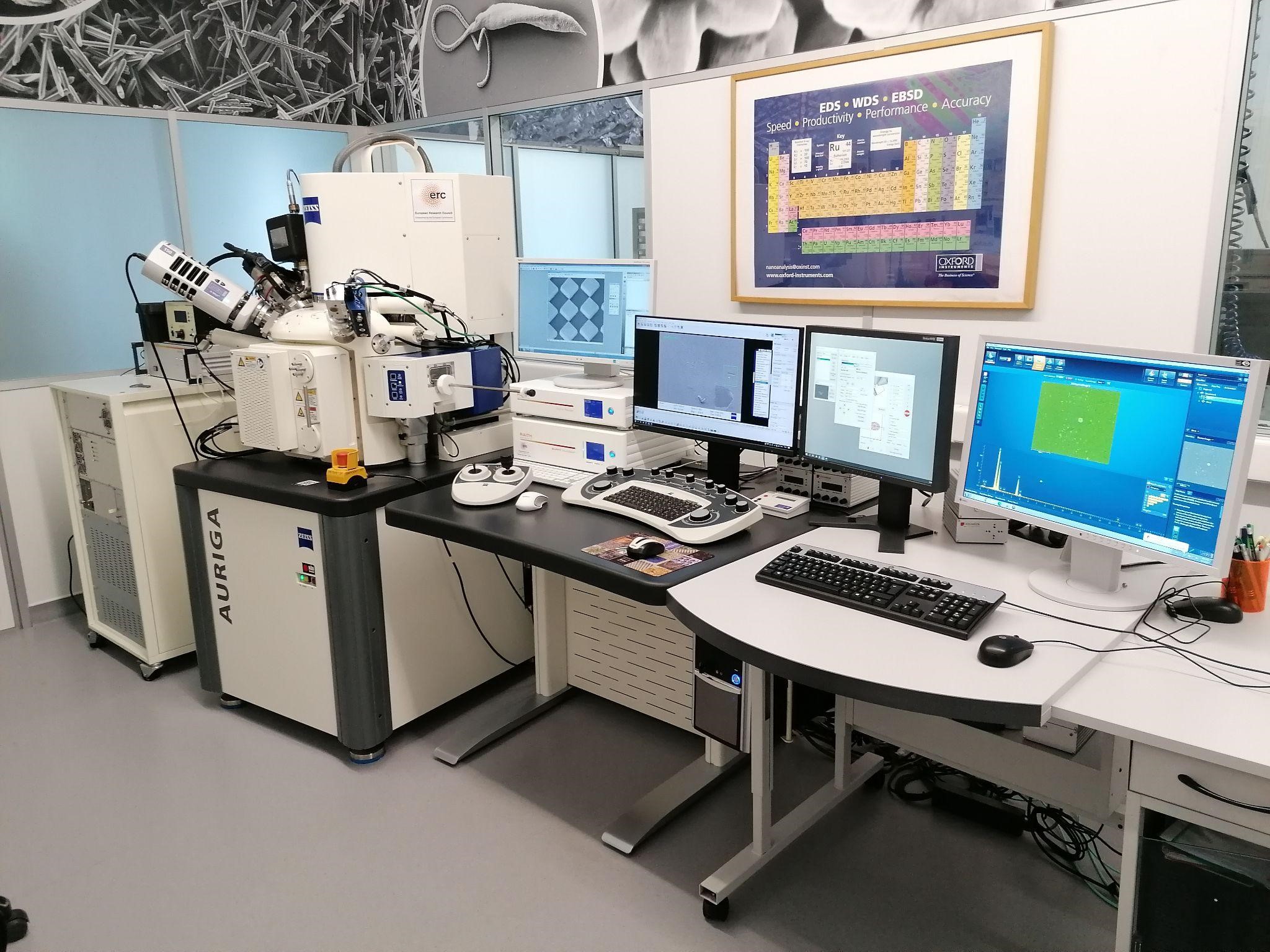
- Carl Zeiss Auriga Crossbeam
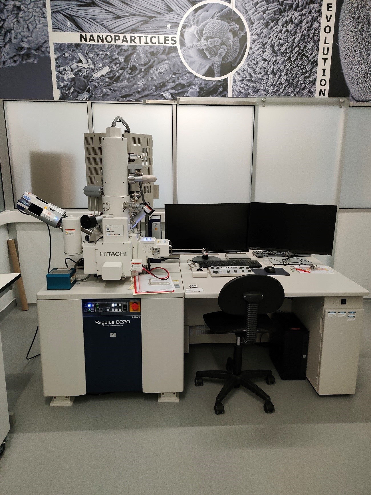
- Hitachi SEM Regulus8220
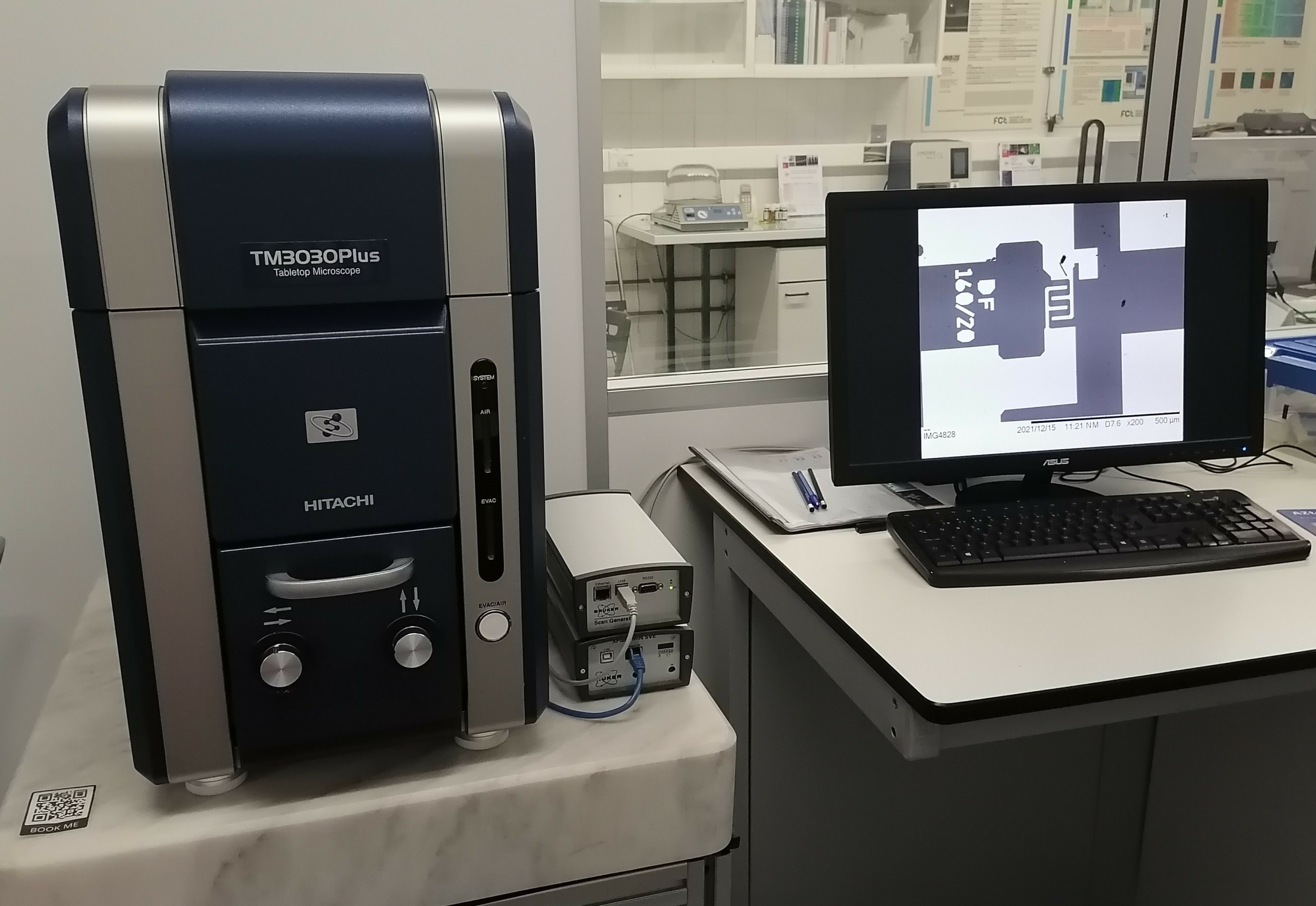
- Hitachi Tabletop TM3030 Plus
Technical specifications:
Carl Zeiss Auriga Crossbeam
- Main technical specifications
- SEM column – Schottky Field Emitter, resolution of 1.0 nm @ 15 kV, 1.9 nm @ 1 kV, acceleration voltage between 0.1 and 30 kV
- FIB column – Ga liquid metal ion source (LMIS), resolution <7 nm @ 30 kV, acceleration voltage between 1 and 30 kV, probe current between 1 pA and 50 nA
- SE and EsB detectors – Everhart-Thornley type SE, In-lens SE and in-lens EsB. Mix-mode possible by tuning grid polarization of detectors
- Large area EDS detector Oxford X-Max 150 with Aztec software for elemental and chemical analysis with high count rates and low beam current. Detection from beryllium (Be) to californium (Cf)
- Microstructure characterization with Oxford Nordlys II-S EBSD, integrated with Aztec software
- Gas injector system for SEM or FIB-assisted local deposition of C, Pt and SiO2, selective etching of dielectrics with XeF2, local charge compensation to reduce charging effects in non-conductive samples
- Heating stage Kammrat & Weiss, for in-situ analysis under heating up to 1050 °C;
- 4 Kleindiek nanotechnik nanomanipulators for electrical measurements of nanodevices and TEM lamela preparation
- Load-lock chamber for fast and contamination free sample loading-unloading.
- Type of samples
- Protocols for preparation of multiple forms of solid samples available (bulk, powder, thin film…), including biological samples (after dehydration)
- Sample size from few mm up to approx 2”.
Hitachi SEM Regulus8220
- Main technical specifications
- Cold field emission (CFE) gun optimized for low-voltage, high-resolution imaging with low aberration: 0.7 nm/1 kV and 0.6 nm/15 kV, and maximum magnification of 2 million times.
- Acceleration voltages from 0.5 to 30 kV.
- Maximum sample height: ≈1 cm, and diameter ≈5 cm.
Hitachi Tabletop TM3030 Plus
- Main technical specifications
- Acceleration voltages of 5 and 15 kV with magnifications of 15x to 60000x.
- Observation modes: BSE:Conductor/Standard/Charge-up Reduction;
- SE:Standard/Charge-up Reduction;
- Mix:Standard/Charge-up Reduction;
- SIGNAL SELECTION: BSE/SE/Mix;
- Maximum sample height: Up to 70mm in diameter and 50mm thickness.
Case study:
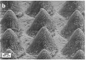
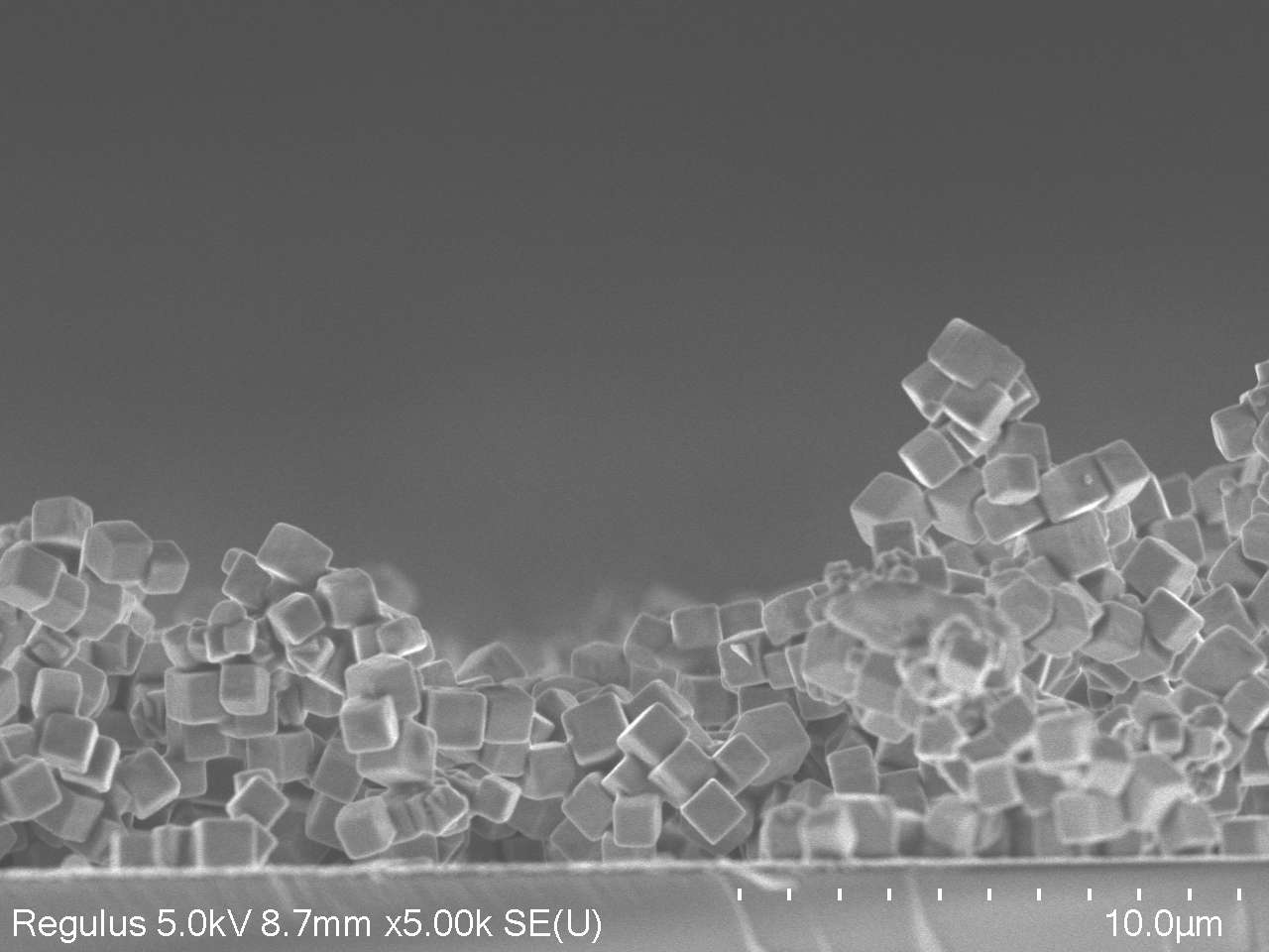
A user will observe his samples using SEM, which allows for high-resolution imaging, and will measure the grain size of his film. After that, the samples will be analysed by EDS for elemental identification and quantification.
Optional:
https://doi.org/10.1021/acsanm.8b00743
Access Provider / Facilities

UNINOVA


