Thin film deposition
About
Layer deposition of metal and dielectric layers using magnetron sputtering and PECVD.
Description
We offer magnetron sputtering of metal and dielectric layers. The PVD system is ideal for both single processes for R&D and small production runs. The system allows up to four materials to be deposited sequentially without removing the sample from the vacuum chamber. Two sputtering modes (RF and DC) allow dielectric and metal layers to be fabricated. Reactive sputtering in a nitrogen and oxygen atmosphere is also possible.
Plasma-Enhanced Chemical Vapour Deposition (PECVD) processes for applications in nanoelectronics, photonics, micromechanics, passivation, encapsulation, and masking. PECVD of silicon oxide, silicon nitrides and silicon oxynitrides with adjustable refractive index. Dielectric multilayer deposition is available.
Technical specifications:
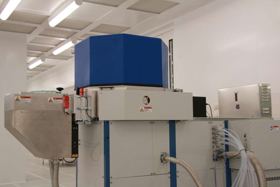
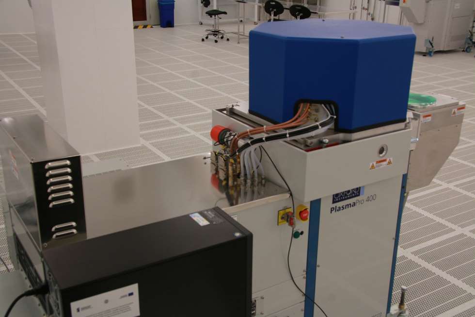
Magnetron sputtering (PlasmaPro 400 Oxford Instruments)
- single substrates with a diameter of up to 200 mm (small pieces also acceptable),
- deposition of Al, Ti, Cr, Mo metal layers and AlN, TiO2, Al2O3, TiN, AlOxNy, TiOxNy (other materials possible by prior arrangement),
- layer thicknesses from a few nanometers to approximately 1 μm,
- magnetrons allowing DC, RF and pulsed DC operation.
PECVD (PlasmaPro 100 Oxford Instruments):
- layer thicknesses from tens of nanometres to single micrometers,
- standard 13.56 MHz RF plasma generator, generator with a frequency range of 50-450 kHz,
- single substrates up to 200 mm in diameter, as well as on smaller substrates of any shape,
• deposition of amorphous silicon (a-Si), silicon oxide (SiOx), silicon nitride (SiNx), and silicon oxynitride (SiOxNy) with controllable composition.
Case study:
A user would like to deposit metal layers for contacts, dielectric layers to fabricate a semiconductor device, fabricate a dielectric layer (SiON) with a targeted refractive index or multi-layer film with desired optical properties.
Access Provider / Facilities