Photolithography
About
Photolithography commonly refers to the pattern transfer of a photomask to a light-sensitive material deposited on a substrate.
Description
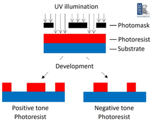
Photolithography, also known as optical lithography or UV lithography, consists in transferring the geometric pattern of a photomask to a UV light-sensitive material (termed as photoresist) deposited onto rigid or flexible substrates. Light exposure induces chemical changes that allow selective dissolution of the exposed (positive tone photoresist) or unexposed (negative tone) regions of the photoresist in a solution called developer. This results in the engraving of the mask pattern or its reverse into the photoresist.
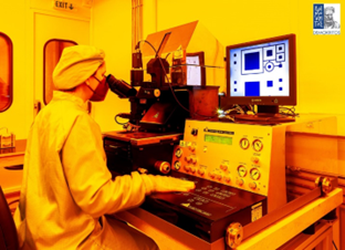
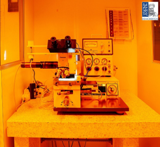
UV exposure is performed using a Mask Aligner that allows high precision mask-to-sample alignment. We offer access to the MJB3 and MA6/BA6 Mask Aligners from SÜSS MicroTec. Different contact exposure modes (vacuum, hard, soft contacts) are available for a sample size up to 4 inch in diameter.
Technical specifications:
- Tools: SÜSS MicroTec MA6/BA6 and KARL SÜSS MJB3 Mask Aligners
- Source / Exposure Wavelength (Band-Pass Filter): 320 nm (MA6/BA6), 365 nm (MJB3)
- Pattern Resolution: 0.8 μm (vacuum contact, MA6/BA6), ~ 1 μm (MJB3)
- Alignment Mode: Top & Back (MA6/BA6) and top (MJB3) side alignment
- Accuracy: ± 0.5 μm (MA6, top side mode), ~ 1 μm (MA6, back side mode), ± 2 μm (MJB3)
- Sample Size: 3” & 4”΄ wafers (4” & 5” masks, MA6/BA6), From 2x2cm2 pieces up to 3” wafers (MJB3)
- Contact Modes: Hard/soft/vacuum contact (MA6/ΒΑ6), Hard/soft (MJB3)
- Additional Tools: Karl Süss RC8 & Headway EC 101D spin-coaters, High-precision hotplate (ATV)
- Environment: Clean-room ISO 6 (Class 1000)
Access Provider / Facilities