SHOWROOM

Welcome to the INFRACHIP showroom!

You will find here all our offer: infrastructures, tools or “know-how” you can get access to.

If you need more specific information, don’t hesitate to contact us.

INFRACHIP provides:

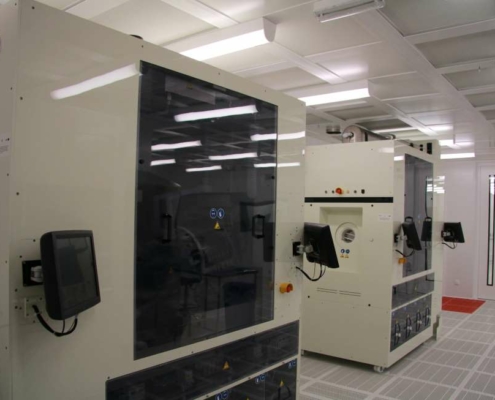
  • A network of approx. 8,000m2 of fully equipped cleanrooms for sensors (nanoelectrochemical, chemical, microfluidics, photonics based sensors, advanced biosensors, graphene enabled),
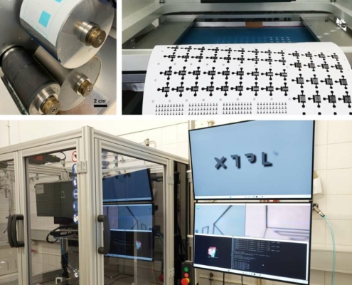
  • manufacturing line for advanced spintronics; Large scale production of organic layers (R2R pilot lines, gravure, slot die, screen printing, etc.);
  • R2R UV nanoimpriting lithography;
  • Laser and plasma assisted vacuum deposition techniques;
  • A wide range of sustainable circuits developed on paper or other recyclable substrates including sensors, TFTs, neuromorphics, energy harvesters and storage, antennas;
  • Full set of tools for processing of devices at high frequencies based on various semiconductor technologies such as SiC, GaAs, InP and GaN;
  • Miniature Wireless Sensor Network (WSN) optimized using a Multi-Paradigm Modelling (MPM) approach;
  • Monolithic microwave integrated circuit (MMIC) processing based on graphene circuits for telecommunications; pilot line for RF front end components (like RF resonators, antennas, etc.);
  • Facilities for the fabrication of flexible, polymer based optical components with free-of-form structure; large scale green inks/pastes production adaptable to various printing technologies;
  • Advanced characterization tools for materials and layers properties evaluation under various conditions; micro-transfer printing for SoC and facilities for hybrid SiP integration.

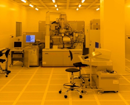
Electron beam lithography

, , , ,
Electron beam lithography is a precise technique for patterning with a nanometer resolution. Th...
Access Provider / Facilities
WUT CEZAMAT

High temperature processes

, , , , , , , , , ,
High-temperature processes (boron diffusion, oxidation, LPCVD, and thermal annealing) in furnac...
Access Provider / Facilities
WUT CEZAMAT

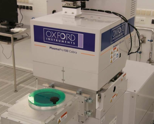
Thin film deposition

, , , , ,
Layer deposition of metal and dielectric layers using magnetron sputtering and PECVD....
Access Provider / Facilities
WUT CEZAMAT

Cleanroom Characterization

, , , , , , , , ,
Myfab Chalmers offers a range of characterization tools for fabricated devices. Scanning electr...
Access Provider / Facilities
Chalmers University

Automatized characterization

, , , , , , ,
Myfab Chalmers offers optical and electron microscopy tools for automatized morphological chara...
Access Provider / Facilities
Chalmers University